RF receiver front-end assembly

a front-end assembly and receiver technology, applied in the direction of waveguide horns, waveguide type devices, electromagnetic transmission, etc., can solve the problems of limited amount of spark gaps, component circuit breakers such as capacitive shunts or capacitive shunts, and the adverse effect of high-energy electromagnetic fields incident on communication radios. , to achieve the effect of increasing optical link gain and enhancing modulation depth

Inactive Publication Date: 2014-06-10
HRL LAB
View PDF42 Cites 6 Cited by
  • Summary
  • Abstract
  • Description
  • Claims
  • Application Information

AI Technical Summary

Benefits of technology

[0024]The disclosed assembly uses a linear array of optoelectronic modulators that are electrically coupled to a linear array of RF waveguides, an example of which is a dielectric filled TEM waveguide. The optical signals in the modulators travel in a direction orthogonal to the direction an RF signal travels in the RF waveguide. Each RF waveguide is part of a multi-furcation of a larger RF waveguide that is fed by a single antenna, such as a TEM horn, a dielectric rod or a dish. For a TEM RF waveguide, the top and bottom walls of the TEM waveguide are electrically coupled to the electrodes for the modulators. In one embodiment, modulators in the array can be optically connected in series, or be cascaded, so that the optical signal travels in sequence from one modulator to the next in the array. The depth of modulation can then be enhanced by using different electrical lengths for the RF waveguides feeding the RF signals to different ones of the modulators in the array, in order to keep the RF signal driving the modulation of those modulators phase matched to the modulated optical signal that propagates from one modulator to the next. A single output optical fiber then connects the assembly with the photodetector of the RF-photonic link. In an alternative embodiment, the modulators in the array can be optically connected in parallel such that each modulator receives an unmodulated optical signal from its laser source and each optical signal is modulated the same way by the RF signals supplied in parallel by means of the multi-furcation. These optical signals may come from one or more lasers, and may be at the same or different wavelengths (the general use of parallel optical modulators is described in related U.S. patent application Ser. No. 12 / 176,089, filed on the same date as this application and entitled “Parallel Modulator Photonic Link”. The overall optical link gain is increased because the modulated optical signals from the parallel modulators are detected by one or more photodetectors and summed.

Problems solved by technology

The adverse effect of high-energy electromagnetic (EM) fields incident on communication radios has been known for a long time.
Component circuit breakers such as semiconductor diodes or capacitive shunts and spark gaps are limited in the amount of current / voltage that can be shunted and by their reaction time.
These printed circuit electrodes, because of the high level of their fringing field, cannot withstand a high power RF input.
While this low signal threshold increases the range between the transmitter and the receiver, it also makes these receivers highly susceptible to destruction by high power incident radiation.
Because the depth of modulation of the optical signal in the electro-optic modulator is directly proportional to the electric field strength, the modulation is weakened by the need to keep the top and bottom conductors of the TEM waveguide far apart.

Method used


Image

  • RF receiver front-end assembly
  • RF receiver front-end assembly
  • RF receiver front-end assembly

Examples


Embodiment Construction

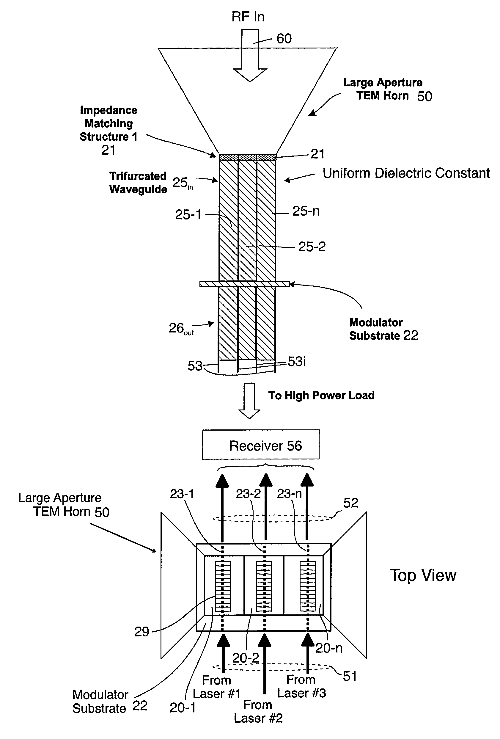
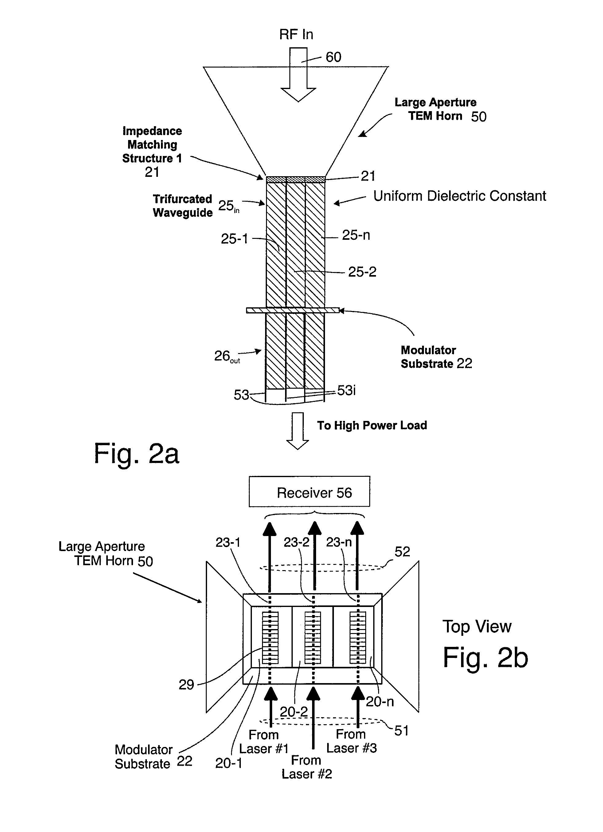
[0048]A first embodiment of this invention wherein multiple optoelectronic modulators are coupled to a single antenna or antenna element is shown in FIGS. 2a and 2b. In these figures, a horn antenna 50 feeds an incident RF electromagnetic signal 60 into a transverse electromagnetic (TEM) multi-furcated RF waveguide 25in (the depicted waveguide is trifurcated, but may have as large a number of furcations or branches as desired). The multiple TEM waveguide sections, i.e., the reduced height TEM waveguides 25-1 through 25-n of the multi-furcated waveguide 25 guide the RF EM field to a modulator substrate 22 that has an array of modulators, or modulator sections, 20-1 through 20-n that are physically oriented parallel to each other. Each modulator 20-1 . . . 20-n contains an optical waveguide 23-1 . . . 23-n. Each modulator also could include an optional grating 29. Each modulator 20-1 . . . 20-n is electrically coupled to an associated reduced-height RF waveguide 25-1 . . . 25-n. Each ...


PUM


Abstract

A waveguide of radio frequency electromagnetic fields is multi-furcated into a plurality of radio frequency waveguide sections, each radio frequency waveguide section having an optoelectronic modulator electrically coupled to it. Each optoelectronic modulator has an optical waveguide disposed therein such that, in use, light traveling in the optical waveguides of the optoelectronic modulators travels in a direction orthogonal with respect to the direction the radio frequency electromagnetic field travels in the radio frequency waveguide sections. The plurality of radio frequency waveguide sections are fed from a common source of said radio frequency energy. In some embodiments, each radio frequency waveguide section has a dielectric material having a length and/or a dielectric constant selected such that a relative time delay of the radio frequency energy propagating in the radio frequency waveguide sections accommodates for a time delay of the light traveling from one optoelectronic modulator to a next optoelectronic modulator of a series connection of multiple optoelectronic modulators.

Description

CROSS REFERENCE TO RELATED APPLICATIONS[0001]This application is related to the following US patent applications: U.S. Ser. No. 12 / 141,825, filed on Jun. 18, 2008 and entitled “Optoelectronic modulator and electric-field sensor with multiple optical-waveguide gratings”; U.S. Ser. No. 12 / 141,834, filed on Jun. 18, 2008 and entitled “Enhanced Linearity RF Photonic Link”; U.S. Ser. No. 12 / 176,089, filed on the same date as this application and entitled “Parallel Modulator Photonic Link”; and U.S. Ser. No. 12 / 176,071, filed on the same date as this application and entitled “Microwave receiver front-end assembly and array”. The disclosures of each of these related applications are hereby incorporated herein by reference.TECHNICAL FIELD[0002]This application discloses a receiver front-end assembly that is sensitive to small radio frequency (RF) signal powers incident upon that assembly, yet is also resistant to damage caused by unwanted high power electromagnetic radiation.BACKGROUND[0003...

Claims


Application Information

Patent Timeline
Patent Type & Authority Patents(United States)
IPC IPC(8): H04B10/80
CPCH04B10/90H01Q13/02H04B2210/006H01P5/12H04B10/80
Inventor SCHAFFNER, JAMES H.YAP, DANIEL
Owner HRL LAB
Why Eureka
Try Eureka