Integrated manufacturing method of semiconductor device

A manufacturing method and semiconductor technology, applied in semiconductor/solid-state device manufacturing, semiconductor devices, electric solid-state devices, etc., can solve the problem of affecting the threshold voltage of P-type semiconductor devices, the thickness limit of P-type metal work function layers, and the influence of thickness on P-type metal Work function layer and other issues

Pending Publication Date: 2021-09-14
SHANGHAI HUALI INTEGRATED CIRCUTE MFG CO LTD
View PDF0 Cites 0 Cited by
  • Summary
  • Abstract
  • Description
  • Claims
  • Application Information

AI Technical Summary

Problems solved by technology

As the size of the device decreases, the metal gate filling groove process will limit the thickness of the P-type metal work function layer.
Therefore, in the prior art, the thicknes

Method used


Image

  • Integrated manufacturing method of semiconductor device
  • Integrated manufacturing method of semiconductor device
  • Integrated manufacturing method of semiconductor device

Examples


Embodiment Construction

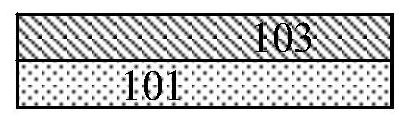
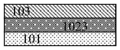
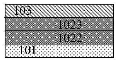
[0066] like Image 6 As shown, it is a flow chart of the integrated manufacturing method of the semiconductor device according to the embodiment of the present invention; in the integrated manufacturing method of the semiconductor device according to the embodiment of the present invention, m kinds of metal work function layers that need to be formed on the semiconductor substrate 301 are integrated. For semiconductor devices, the thickness of the work function layer of the first type of metal decreases gradually from the first type to the mth type of semiconductor device. The steps of forming the first type of metal work function layer with m thicknesses include:

[0067] Step 1. According to the thickness differences of the first-type metal work function layers of various thicknesses, divide the thickest first-type metal work-function layer from bottom to top into the first, second and up to the first m first-type metal work function sublayers.

[0068] Step 2: Perform m c...


PUM


Abstract

The invention discloses an integrated manufacturing method of a semiconductor device. A process of forming first-class metal work function layers with m thicknesses comprises the following steps: 1, dividing the first-class metal work function layer with the thickest thickness into a first first-class metal work function sub-layer, a second first-class metal work function sub-layer to an mth first-class metal work function sub-layer from the bottom to the top; and 2, carrying out m times of circulation processes, wherein each time of circulation process comprises a metal work function comprehensive deposition process and a metal work function selective etching process. Each circulation process is set as follows: first to mth first-class metal work function sub-layers are sequentially formed in each metal work function comprehensive deposition process; and the etching area of each time of metal work function selective etching process is reduced in sequence so as to ensure that each time of metal work function selective etching process only etches one independent first type of metal work function sub-layer. According to the invention, undercutting at the bottom of the thicker first type metal work function layer can be avoided, so that the metal work function boundary effect can be optimized.

Description

technical field [0001] The invention relates to a method for manufacturing a semiconductor integrated circuit, in particular to an integrated method for manufacturing a semiconductor device. Background technique [0002] With the development of semiconductor technology, a metal gate (MG) is usually used in the gate structure of a semiconductor device with a high process node, and a high dielectric constant layer (HK) is usually used as a gate dielectric layer, and HK and MG are stacked to form an HKMG structure. [0003] As the size of the semiconductor device is further reduced, the semiconductor device will adopt a fin-type transistor structure, the fin-type transistor includes a fin body, the fin body is in a nano-strip or nano-sheet structure, and the fin body is formed by the semiconductor substrate bottom etched. The gate structure covers a portion of the length of the top surface and sides of the fin body. The source region and the drain region are formed in the fin...

Claims


Application Information

Patent Timeline
IPC IPC(8): H01L27/088H01L21/336
CPCH01L27/0886H01L29/66795
Inventor 翁文寅
Owner SHANGHAI HUALI INTEGRATED CIRCUTE MFG CO LTD
Why Eureka
Try Eureka