A peCVD device for preparing amoled

An inner cavity and cavity technology, which is applied in the field of PECVD equipment, can solve the problems of increased cost of cavity components, deterioration of aluminum stiffness/strength, softening and other problems, so as to ensure the quality of film formation, reduce production costs, and simplify the overall design effect

Active Publication Date: 2018-03-27
IDEAL ENERGY SHANGHAI SUNFLOWER THIN FILM EQUIP
View PDF6 Cites 0 Cited by
  • Summary
  • Abstract
  • Description
  • Claims
  • Application Information

AI Technical Summary

Problems solved by technology

[0004]The melting point of general aluminum is 580-700°C, when the aluminum used to prepare the PECVD reaction chamber is heated above 350°C, the aluminum Stiffness / strength will be significantly worse, and even softening will occur, which will seriously affect the quality of deposited film in the reaction chamber. At this time, the traditional thickness of the aluminum chamber will no longer be suitable for the production of AMOLED reaction chamber
In order to meet the rigidity / strength requirements of the reaction chamber, some manufacturers will increase the thickness of the aluminum material by 5-7 times, which will undoubtedly cause a linear increase in the cost of the chamber material and increase the volume of the chamber, especially for those with inner chambers and For PECVD equipment with an external cavity, the volume of the vacuum environment also increases accordingly, which requires the use of a higher power vacuum pump, resulting in an increase in the cost of cavity components
At the same time, the huge reaction chamber also brings many difficulties to processing and transportation

Method used


Image

  • A peCVD device for preparing amoled
  • A peCVD device for preparing amoled
  • A peCVD device for preparing amoled

Examples


Embodiment Construction

[0043]In order to make the above objects, features and advantages of the present invention more comprehensible, specific implementations of the present invention will be described in detail below in conjunction with the accompanying drawings.

[0044] In the following description, many specific details are set forth in order to fully understand the present invention, but the present invention can also be implemented by other methods different from those described here, so the present invention is not limited by the specific embodiments disclosed below.

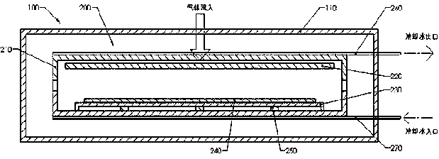
[0045] figure 1 It is a schematic structural diagram of a PECVD device for preparing AMOLED provided by the present invention, the PECVD device includes an outer cavity 100 providing a vacuum environment and an inner cavity 200 for performing a plasma-enhanced chemical vapor deposition reaction, the outer cavity 100 The cavity can be made of high-temperature-resistant metal materials such as aluminum or stainless steel, and th...


PUM


Abstract

The invention provides a PECVD device for preparing AMOLED; and through a series of technical means that a vacuum environment external cavity is combined with an inner cavity for performing a plasma enhanced type chemical vapor deposition reaction, a base plate is subjected to 400-450 DEG C local direct high temperature heating, an interval component is adopted and cooling mechanisms are respectively arranged at the top wall and the bottom wall of a cavity body, a technical effect that a high-temperature AMOLED process is carried out by adopting a low-temperature PECVD reaction cavity is achieved, and the problems that because aluminum is used as a cavity body material of a reaction cavity in a traditional way, the material has the strength and the rigidity becoming poor and generates severe thermal deformation when facing a 400-450 DEG C high temperature environment are solved.

Description

Technical field: [0001] The invention relates to the field of AMOLED process equipment, in particular to a PECVD device for preparing AMOLED. technical background: [0002] In traditional industries such as solar energy and LCD flat panel display industries, the process temperature required to prepare nitride films, oxide films, amorphous / microcrystalline silicon films and other films by PECVD (plasma enhanced chemical vapor deposition) is usually 200-280 °C . In these PECVD equipment, due to the use of NF3 gas for cleaning and the high-temperature atmosphere in the reaction chamber during the film deposition process, the chamber material must have good anti-fluorine gas corrosion characteristics and excellent high-temperature performance. Currently, metals that meet these conditions Materials are aluminum, nickel, tantalum and titanium alloys. Among them, nickel, tantalum and titanium alloys are difficult to process into large sizes due to the limitation of the technology...

Claims


Application Information

Patent Timeline
IPC IPC(8): C23C16/44
Inventor 杨飞云谭晓华陈金元徐升东李朋李一成刘传生
Owner IDEAL ENERGY SHANGHAI SUNFLOWER THIN FILM EQUIP
Why Eureka
Try Eureka