Thin film transistor, method of manufacturing thin film transistor, and manufacturing system

a manufacturing system and thin film technology, applied in the field of thin film transistors, can solve problems such as the decrease of achieve the effects of increasing the electrical reliability of the device, high resistance, and improving the boundary

Active Publication Date: 2020-07-16
WUHAN CHINA STAR OPTOELECTRONICS TECH CO LTD
View PDF0 Cites 0 Cited by
  • Summary
  • Abstract
  • Description
  • Claims
  • Application Information

AI Technical Summary

Benefits of technology

[0046]The embodiments of the present application provide a thin film transistor, a method of manufacturing a thin film transistor, and a manufacturing system. The thin film transistor includes a substrate, a buffer layer, an active layer, and a gate insulating layer. After a silicon island pattern is formed on the active layer, a side area of the active layer not protected by a photoresist is doped and modified though an ion implantation doping technique, so that a surface of the side area is formed as a high resistance area, and then the gate insulating layer is formed by a chemical deposition process. Because a side surface of the active layer tilts at a certain inclined angle after being formed dry etching, the gate insulating layer deposited on the side surface of the active layer is thinner than other portions of the gate insulating layer. Forming the side area of the active layer as a high-resistance structure can avoid a weak channel current produced by an unintentional electrically conduction of a boundary of the active layer due to a thinner thickness of the gate insulating layer when operating, thereby improving boundary effect and increasing electrical reliability of the device.

Problems solved by technology

When a thin film transistor (TFT) is operating, an area where the gate insulating layer 202 is located is unintentionally electrically conducted in advance and produces a weak channel current, causing a hump effect, and resulting in a decrease in electrical reliability of devices.

Method used


Image

  • Thin film transistor, method of manufacturing thin film transistor, and manufacturing system
  • Thin film transistor, method of manufacturing thin film transistor, and manufacturing system
  • Thin film transistor, method of manufacturing thin film transistor, and manufacturing system

Examples


Embodiment Construction

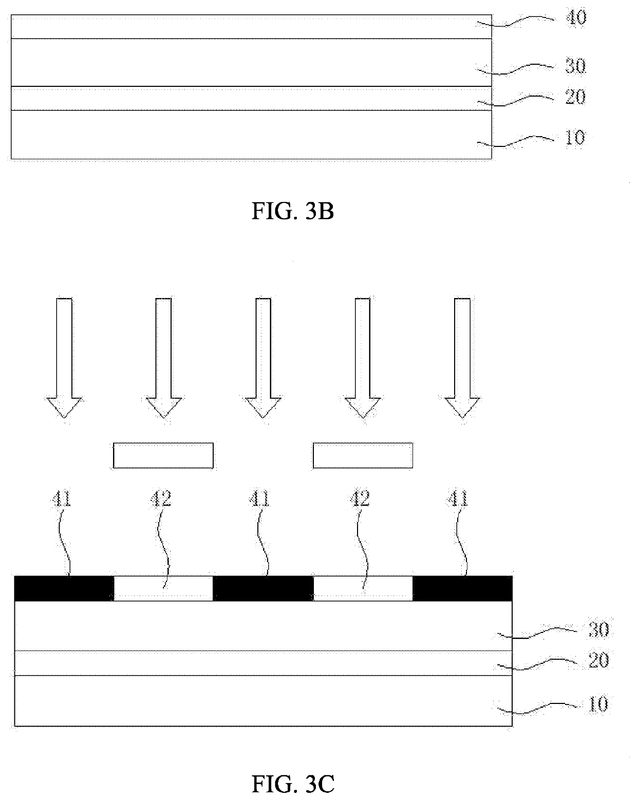
[0052]The following embodiments are referring to the accompanying drawings for exemplifying specific implementable embodiments of the present disclosure. Furthermore, directional terms described by the present disclosure, such as upper, lower, front, back, left, right, inner, outer, side, etc., are only directions by referring to the accompanying drawings, and thus the used directional terms are used to describe and understand the present disclosure, but the present disclosure is not limited thereto. In the drawings, elements with similar structures are labeled with like reference numerals.

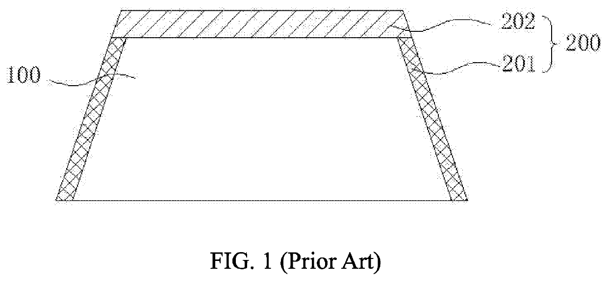
[0053]The present application is directed to a hump effect caused by a thinner gate insulating layer formed at a silicon island boundary of an existing thin film transistor, and this embodiment can mitigate the hump defect.

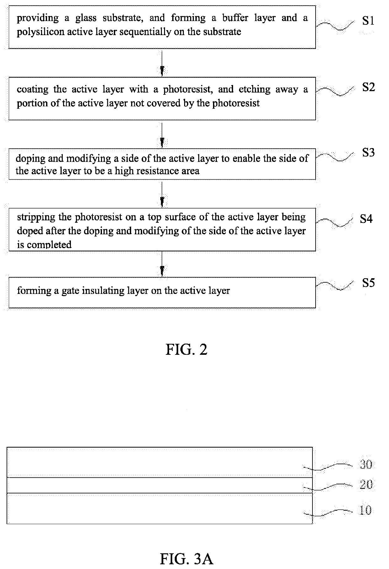
[0054]As shown in FIG. 2, a specific embodiment of the present application provides a method of manufacturing a thin film transistor, and the method includes steps as follows:

[0...


PUM

PropertyMeasurementUnit
energyaaaaaaaaaa
resistanceaaaaaaaaaa
resistance areaaaaaaaaaaa

Abstract

The present application provides a thin film transistor, a method of manufacturing a thin film transistor, and a manufacturing system. The thin film transistor includes a substrate, a buffer layer, an active layer, and a gate insulating layer. A side area of the active layer is doped and modified, so that a surface of the side area is formed as a high resistance area, and then the gate insulating layer is formed by a chemical deposition process, thereby to avoid a weak channel current produced by unintentional electrically conduction of a boundary of the active layer due to a thinner thickness of the gate insulating layer when operating, thereby increasing electrical reliability of the thin film transistor.

Description

BACKGROUND OF INVENTION1. Field of Invention[0001]The present application relates to a display field, and particularly, to a thin film transistor, a method of manufacturing a thin film transistor, and a manufacturing system.2. Related Art[0002]In order to avoid display defects caused by a large leakage current, conventional low temperature poly silicon-thin film transistors (LTPS-TFTs) are generally configured with a top gate structure, using a self-aligned feature to fabricate a lightly doped drain (LDD) structure to reduce a leakage current in channels. As shown in FIG. 1, in actual production, since LTPS-TFTs are formed by a dry etching process to form a silicon island pattern, when a gate insulating layer 200 is formed on a silicon island 100 by a chemical vapor deposition process, a gate insulating layer 201 formed on a side area of the silicon island 100 is thinner, but a gate insulating layer 202 formed on a top area of the silicon island 100 is thicker. When a thin film tran...

Claims


Application Information

Patent Timeline
Patent Type & Authority Applications(United States)
IPC IPC(8): H01L29/66H01L29/786H01L21/265
CPCH01L29/78642H01L29/66757H01L21/26513H01L21/26506H01L29/42384H01L29/78675H01L29/78609
Inventor NIE, XIAOHUIZHANG, JIAWEI
Owner WUHAN CHINA STAR OPTOELECTRONICS TECH CO LTD
Why Eureka
Try Eureka