
Test device and test method for mobile phone PCB board

A PCB board and testing device technology, applied in the field of circuit testing, can solve problems such as high probe unit price and increased production costs

Active Publication Date: 2022-07-08
广州弘高科技股份有限公司
View PDF14 Cites 0 Cited by
  • Summary
  • Abstract
  • Description
  • Claims
  • Application Information

AI Technical Summary

Problems solved by technology

[0009] The improvement direction of the above-mentioned patents is to improve the probe of the flying probe device into a split probe connected by an elastic member, or the middle part of the probe is elastic, or the probe is installed on the elastic member, which are all opposite to the probe. The improvement of the needle, so that the unit price of the probe is getting higher and higher
and the probe is a consumable part, which greatly increases the production cost by improving the design of the probe to achieve a soft landing

Method used


Image

  • Test device and test method for mobile phone PCB board
  • Test device and test method for mobile phone PCB board
  • Test device and test method for mobile phone PCB board

Examples


Embodiment 1

[0045] Because the probe is a consumable part, improving the probe will make the unit price of the probe higher and higher, and the cost of using the equipment will also increase. Soft landing is a problem that needs to be solved urgently. One of the solutions is to reduce the contact speed between the probe and the PCB board. However, reducing the moving speed of the probe will reduce the working frequency of the probe, thereby affecting the test efficiency.

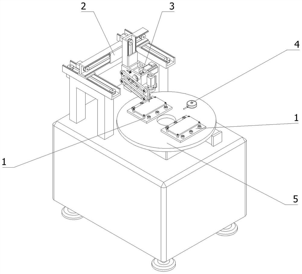
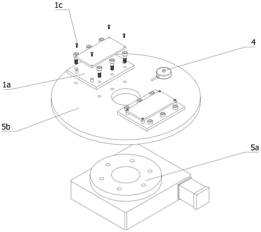
[0046] In order to solve this technical problem, such as Figure 1-3 shown, provide:

[0047] A test device for a mobile phone PCB board, comprising,

[0048] frame;

[0049] Fixture 1, which is set on the rack, and fixture 1 is used for positioning the PCB board;

[0050] Industrial robot 2, which is arranged on the rack;

[0051] The flying probe test shaft 3 is arranged at the output end of the industrial robot 2, and the flying probe test shaft 3 is used for circuit testing the PCB board;

[0052] Flying probe ...

Embodiment 2

[0089] Since the movement trajectory of the free end of the first rocker arm 3d is an arc, it is difficult to calculate the angle of the detection end of the probe module 3e when the detection end of the probe module 3e is in contact with the PCB board. In order to solve this technical problem, such as Figure 8 and 9 As shown, the following preferred technical solutions are provided:

[0090] Flying probe test shaft 3 also includes,

[0091] The second rocker arm 3g, one end of which is mounted on the mounting frame 3a through a rotating pair, and the second rocker arm 3g is parallel to the first rocker arm 3d;

[0092] The two ends of the connecting rod 3h are respectively hinged with the free end of the first rocker arm 3d and the free end of the second rocker arm 3g, and the probe module 3e is installed on the connecting rod 3h.

[0093] Specifically, the mounting bracket 3a, the first rocker arm 3d, the second rocker arm 3g and the connecting rod 3h constitute a paralle...


PUM


Abstract

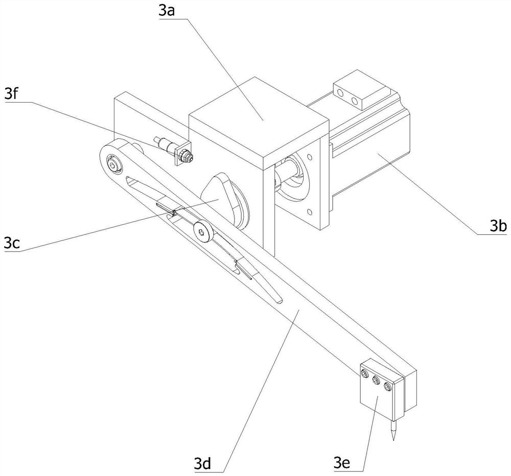
The invention relates to the field of circuit testing, in particular to a testing device for a mobile phone PCB board. The test device includes a frame, a fixture, an industrial robot; a mounting frame, which is arranged at the output end of the industrial robot; a motor, which is mounted on the mounting frame; an eccentric shaft, one end of which is coaxially mounted on the output shaft of the motor; the first The rocker arm, one end of which is installed on the mounting frame through the rotating pair, the middle part of the first rocker arm is provided with a chute, the longitudinal direction of the chute is parallel to the length direction of the first rocker arm, and the other end of the eccentric shaft is inserted in the slide. The groove is inside and slidingly matched with the chute; the probe module is arranged on the free end of the first rocker arm; the controller is used for collecting test data of the probe module. In the present application, the speed of the probe module approaching the PCB board is reduced by the quick return mechanism, and the lower half of the first rocker arm is made of elastic material, so as to realize the slow soft landing of the probe module without reducing the work of the probe module frequency.

Description

technical field [0001] The invention relates to the field of circuit testing, in particular to a testing device for a mobile phone PCB board. The invention also relates to a testing method of a testing device of a mobile phone PCB board. Background technique [0002] At present, there are two main methods for PCB electrical testing: one is the bed of needles in-circuit test (ICT), and the other is the flying probe test. Although the test efficiency of the flying probe test system is slightly inferior to that of the ICT test, the flying probe test system has the advantages of rapidity, economy and flexibility compared with the online test of the needle bed. [0003] Subject to the constraints of the solder joint spacing, for some high-density PCB boards, the coverage rate of the needle bed test can only reach 60% to 70%, while the flying probe test system is based on the network logic relationship of the PCB board. The probe is used for testing, and the probe has a certain ...

Claims


Application Information

Patent Timeline
Patent Type & Authority Patents(China)
IPC IPC(8): G01R31/28G01R1/067G01L1/22G05D15/01
CPCG01R31/2808G01R1/06722G01L1/22G05D15/01
Inventor 王辉杨鹏
Owner 广州弘高科技股份有限公司
Learn More