Polishing pad and manufacturing method of semiconductor device

A manufacturing method and polishing pad technology, applied in the field of polishing pads, can solve problems such as lack of in-depth research, influence on the manufacturing process of semiconductor devices, insufficient research, etc., and achieve excellent polishing performance

Active Publication Date: 2021-10-22
HUBEI DINGHUI MICROELECTRONICS MATERIALS CO LTD +1
View PDF5 Cites 0 Cited by
  • Summary
  • Abstract
  • Description
  • Claims
  • Application Information

AI Technical Summary

Problems solved by technology

[0006] Various forms of groove structures are disclosed in the prior art, but there is no in-depth study on the relationship between the specific groove structure and polishing performance and how to optimize it. As an experimental science, the research on polishing performance has co

Method used


Image

  • Polishing pad and manufacturing method of semiconductor device
  • Polishing pad and manufacturing method of semiconductor device
  • Polishing pad and manufacturing method of semiconductor device

Examples


Example Embodiment

[0076] Embodiment

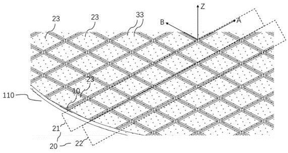
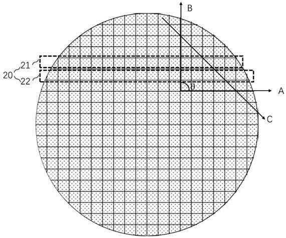
[0077] figure 1 It is an exemplary display according to a polishing pad of a polishing pad according to an embodiment of the present invention, a plan view of a polishing pad. figure 2 . In order to make it easy to explain, figure 1 The first direction is referred to as a direction, and the second direction is referred to as a B direction, and the third direction is referred to as a C direction, and the polishing pad thickness direction, that is, the direction perpendicular to the surface of the polishing pad is referred to as the Z direction.

[0078] In an embodiment, the direction A direction is 90 degrees in the direction, i.e., SIN θ is 1. Refer figure 1 The polishing pad of the present invention is suitable for polishing or planating at least one of a semiconductor, an optical, and a magnetic substrate. The polishing layer 110 has a polishing surface 10 and a polishing unit group 20, and the polishing unit group 20 is distributed over the polishing surfa...

Example Embodiment

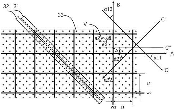
[0114] According to an embodiment of the present invention, the first direction is 90 ° in the second direction; the third direction is not α1 with an angle in the first direction, the α1 The range is 10 ° ≤ α1 ≤ 45 °; and / or, the third direction is α2 in the third direction to the second direction, and the α2 has a range of 10 ° ≤ α2 ≤ 45 °.

[0115] As a more preferred embodiment of the present invention, the first direction is 90 ° in the first direction, 90 °; the third direction is α1 in the third direction and the first direction is α1, said The α1 ranges from 10 ° ≤ α1 ≤ 20 °; and / or the third direction is α2 with the upper portion of the second direction, and the α2 ranges from 10 ° ≤ α2 ≤ 20 °.

[0116] An embodiment of the present invention discloses the center of a pit of the first pit set and a triangular V. More preferably, equilateral triangles.

[0117] More preferably, the triangular V is an equilateral triangle, and the angle θ of the first direction is 90 ° i...

Example Embodiment

[0118] Embodiment 2

[0119] Similar to the embodiment, the direction in the second embodiment is 90 degrees in the direction in the direction, i.e., SIN θ is 1. Similarly, the three-dimensional structure of the independent polishing unit can be referenced figure 1 The polishing layer has a polishing surface and a polishing unit group, and the polishing unit group is distributed on the polishing surface, and the surface of the polishing unit group is directly in contact with the abrasive material.

[0120] Reference style of polishing unit of polishing layer Figure 9 The first portion 41 and the second portion 42 of the second portion 42 are interleaved distribution. Preferably, the disturbed distance is half the edge length of the grinding unit in the A direction.

[0121] This embodiment is one of the preferred embodiments of the present invention, similarly, and evenly distributed pits 53, the size of the polishing unit, the shape, size, and size of the pits are as defined as d...


PUM


Abstract

The invention discloses a manufacturing method of a semiconductor device. The method comprises the process of grinding the surface of a semiconductor wafer by using a polishing pad with a specific pattern. The invention further discloses the polishing pad. The polishing pad comprises a polishing layer, the polishing layer comprises a polishing surface and polishing units located on the polishing surface, one ends of the polishing units form a contact surface, and the contact surface is in direct contact with a ground material. The multiple polishing units form first parts and second parts respectively, the first parts extend in a first direction and are evenly spaced, and the second parts extend in a direction parallel to the first direction and are evenly spaced. The polishing layer is further provided with pits, including the first part of pits and the second part of pits. The polishing pad has excellent comprehensive performance when parameters such as the polishing unit area ratio, the pit area ratio and the volume ratio are limited to be in a proper range.

Description

technical field [0001] The invention relates to the field of chemical mechanical polishing (CMP) of semiconductors, in particular to a polishing pad for polishing at least one of a magnetic substrate, an optical substrate and a semiconductor substrate, and having a well-designed surface pattern structure And a manufacturing method for polishing a semiconductor device using the polishing pad. Background technique [0002] In the manufacturing and processing of integrated circuits, other electronic devices and optical materials, many materials are involved in polishing, thinning or planarization, among which chemical mechanical polishing is the most widely used. The principle of chemical mechanical polishing is that on a fixed polishing machine, the abrasive liquid is applied to the polishing pad. The polishing pad contacts the surface of the material to be ground, and a chemical reaction will occur. At the same time, the polishing pad and the material to be ground are process...

Claims


Application Information

Patent Timeline
IPC IPC(8): B24B37/22B24B37/24B24B37/26B24B37/005B24B49/00H01L21/3105
CPCB24B37/22B24B37/24B24B37/26B24B37/005B24B49/006H01L21/31053
Inventor 黄学良邱瑞英杨佳佳张季平朱顺全
Owner HUBEI DINGHUI MICROELECTRONICS MATERIALS CO LTD
Why Eureka
Try Eureka