On-chip cache device and read-write method

An on-chip cache and high-speed cache technology, applied in the field of communication chips, can solve the problems of large chip storage area, waste of storage space, and high power consumption, and achieve the effects of improving utilization, reducing power consumption, and reducing storage area

Pending Publication Date: 2021-10-22
SANECHIPS TECH CO LTD
View PDF0 Cites 8 Cited by
  • Summary
  • Abstract
  • Description
  • Claims
  • Application Information

AI Technical Summary

Problems solved by technology

[0003] In the existing chip design, the resource space of the chip is used in different ways in different application scenarios. In the big data processing scenario, due to the generation of small packets, the storage in the chip can only be stored by row address, and the chip processes small packets. At this time, each row address can only store a small packet message, which wastes a lot of storage space. In order to process the small packet message, the chip design has a large storage area, resulting in the problem of high power consumption.

Method used


Image

  • On-chip cache device and read-write method
  • On-chip cache device and read-write method
  • On-chip cache device and read-write method

Examples


Embodiment Construction

[0017] In order to make the purpose, technical solution and advantages of the application clearer, the embodiments of the application will be described in detail below in conjunction with the accompanying drawings. It should be noted that, in the case of no conflict, the embodiments in the present application and the features in the embodiments can be combined arbitrarily with each other.

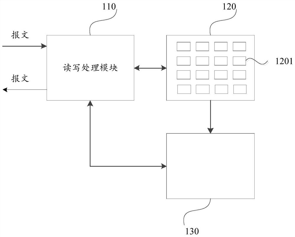
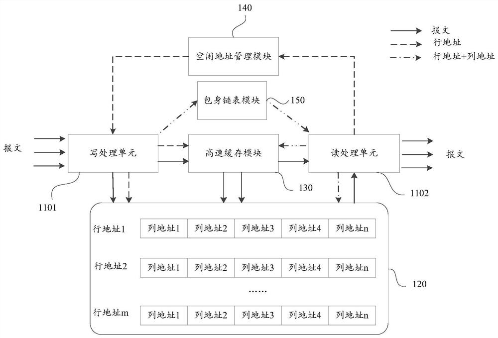
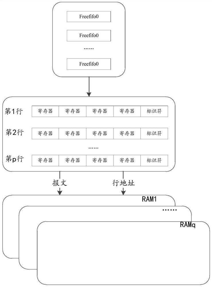
[0018] Since the memory in the chip stores messages according to the row address, each row in the memory stores only one message. When the chip is used for processing large amounts of data, the length of the message is less than For ordinary messages, when the chip writes and reads small packets and long messages, a large amount of storage space is wasted on the chip memory. Correspondingly, a larger memory needs to be installed on the chip, and the chip area is larger and the power consumption is too high. In this embodiment of the present application, multiple small packets and long messa...


PUM


Abstract

The invention provides an on-chip cache device and a read-write method, and the device comprises a read-write processing module, a high-speed cache module and a memory module, wherein the read-write processing module is respectively connected with the cache module and the memory module, and the read-write processing module is used for storing messages in the cache module and the memory module, reading the messages stored in the cache module and the memory module, and transferring the messages cached in the cache module to the memory module; the high-speed cache module is connected with the memory module through the read-write processing module, and the high-speed cache module comprises at least one cache register and is used for temporarily caching messages; and the memory module is connected with the read-write processing module and is used for transferring the message cached by the high-speed cache module. The multiple messages are cached to be written into the buffer at the same time, the chip storage space utilization rate is increased, the storage area is reduced, and chip power consumption is reduced.

Description

technical field [0001] The present application relates to the field of communication chips, in particular to an on-chip cache device and method. Background technique [0002] In the network switching engine, due to the requirements of performance index improvement and the limitation of chip area, resources and industry, it is impossible for the chip to meet the demand of performance improvement by increasing the main frequency and stacking resources without limit, so an implementation is urgently needed. The low redundancy of chip space and low area consumption realize the improvement of chip performance. [0003] In the existing chip design, the resource space of the chip is used in different ways in different application scenarios. In the big data processing scenario, due to the generation of small packets, the storage in the chip can only be stored by row address, and the chip processes small packets. At this time, each row address can only store a small packet message, ...

Claims


Application Information

Patent Timeline
Patent Type & Authority Applications(China)
IPC IPC(8): G06F15/78G06F3/06
CPCG06F15/7846G06F3/0656G06F3/0626Y02D10/00G11C5/04G11C11/4076G11C11/408G11C2207/2245G06F12/0824G06F12/0868G06F13/1673
Inventor 梁苇超仲建锋胡达陈昌胜徐东国陆健锋
Owner SANECHIPS TECH CO LTD
Why Eureka
Try Eureka