Liquid crystal display panel and display device

A technology for liquid crystal display panels and non-display areas, applied in instruments, nonlinear optics, optics, etc., can solve problems such as weak antistatic ability and electrode damage

Active Publication Date: 2022-05-06
HKC CORP LTD
View PDF5 Cites 0 Cited by
  • Summary
  • Abstract
  • Description
  • Claims
  • Application Information

AI Technical Summary

Problems solved by technology

[0004] The purpose of the embodiments of the present application is to provide a liquid crystal display panel and a display device. By setting the distance between the first electrode layer of the color filter substrate and the second electrode layer of the array substrate as a safe distance without arc discharge, Solve the problem that the antistatic ability of the existing liquid crystal display panel is weak and the electrodes are easily damaged

Method used


Image

  • Liquid crystal display panel and display device
  • Liquid crystal display panel and display device
  • Liquid crystal display panel and display device

Examples


Embodiment 1

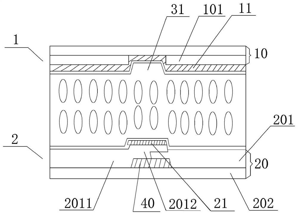
[0049] refer tofigure 1 , the liquid crystal display panel provided in Embodiment 1 of the present application includes a color filter substrate 1 and an array substrate 2;

[0050] The color filter substrate 1 includes a first base substrate 10 and a first electrode layer 11 arranged on the first base substrate 10; the array substrate 2 includes a second base substrate 20 and an electrode layer arranged on the second base substrate 20. The second electrode layer 21 ; the distance between the second electrode layer 21 and the first electrode layer 11 is greater than or equal to the threshold; the threshold is a critical safety distance for arc discharge between the first electrode layer 11 and the second electrode layer 21 .

[0051] With the liquid crystal display panel provided in the embodiment of the present application, the distance between the first electrode layer 11 of the color filter substrate 1 and the second electrode layer 21 of the array substrate 2 is set to be g...

Embodiment 2

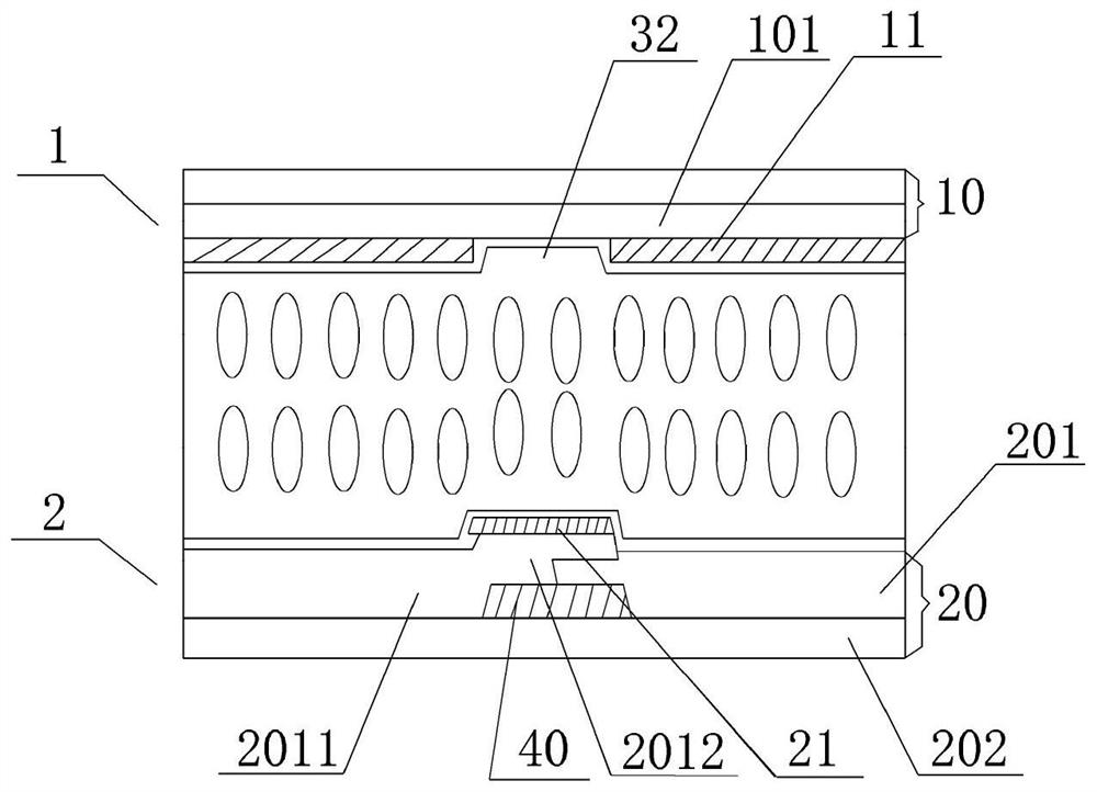
[0066] refer to figure 2 , in the second embodiment of the present application, the second groove 32 is provided on the surface of the first electrode layer 11 facing the array substrate 2; the orthographic projection of the second groove 32 on the second base substrate 20 is located at the second The electrode layer 21 is in an orthographic projection on the second base substrate 20 .

[0067] Since arc discharge occurs between the first electrode layer 11 and the second electrode layer 21, a second groove 32 may be provided on the surface of the first electrode layer 11 facing the array substrate 2, and the second groove The orthographic projection of 32 on the second base substrate 20 is located within the orthographic projection of the second electrode layer 21 on the second base substrate 20, so that the position corresponding to the second electrode layer 21 on the first electrode layer 11 is The second groove 32, the depth of the second groove 32 can increase the dist...

Embodiment 3

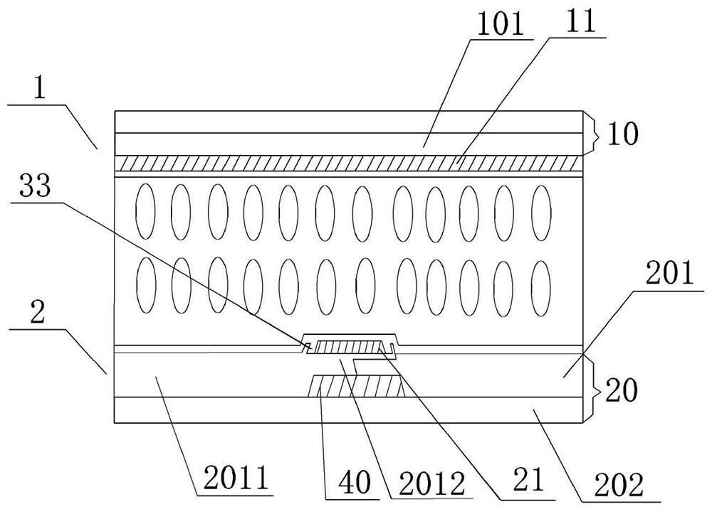
[0071] refer to image 3 , in Embodiment 3 of the present application, a third groove 33 is formed on the second base substrate 20 ; the second electrode layer 21 is located in the third groove 33 .

[0072] In this application, in addition to setting the first groove 31 on the first base substrate 10 or setting the second groove 32 on the first electrode layer 11 to increase the distance between the first electrode layer 11 and the second electrode layer 21 distance, a third groove 33 can also be set on the second base substrate 20, so that the second electrode layer 21 is located in the third groove 33, so that the depth of the third groove 33 can increase the first The distance between the electrode layer 11 and the second electrode layer 21 prevents arc discharge between the first electrode layer 11 and the second electrode layer 21 .

[0073] It should be noted that the depth of the third groove 33 should meet the requirement that the distance between the first electrode...


PUM


Abstract

The present application provides a liquid crystal display panel and a display device. The liquid crystal display panel includes a color filter substrate and an array substrate, and the color filter substrate includes a first base substrate and a first electrode layer disposed on the first base substrate. , the array substrate includes a second base substrate and a second electrode layer disposed on the second base substrate, the distance between the second electrode layer and the first electrode layer is greater than or equal to a threshold; The threshold is a critical safety distance for arc discharge between the first electrode layer and the second electrode layer. The application solves the problem that the antistatic ability of the existing liquid crystal display panel is weak and the electrodes are easily damaged.

Description

technical field [0001] The present application belongs to the field of display technology, and more specifically relates to a liquid crystal display panel and a display device. Background technique [0002] At present, in order to increase the aperture ratio of the liquid crystal panel in use, the common practice in the industry is to make the RGB (red, green and blue) color resistors on the TFT (thin film transistor) side, overlap two adjacent color resistors, and set the data lines on the Where the color resistance overlaps, a layer of shielding electrode is designed on the surface of the color resistance overlap, that is, above the data line to shield the parasitic capacitance between the data line and the electrode on the color filter substrate. [0003] However, since the shielding electrode extends from the display area to the non-display area along the data line, the non-display area has a light-shielding layer, and the height of the color-resistor overlap is greater ...

Claims


Application Information

Patent Timeline
Patent Type & Authority Patents(China)
IPC IPC(8): G02F1/1333G02F1/1343
CPCG02F1/1333G02F1/1343G02F1/134309G02F2202/22G02F1/136204G02F1/133512G02F1/133514G02F1/136286G02F2201/50
Inventor 黄世帅郑浩旋
Owner HKC CORP LTD
Why Eureka
Try Eureka