

Semiconductor testing equipment
A testing equipment and semiconductor technology, applied in the direction of electronic circuit testing, measuring electricity, measuring devices, etc., can solve the problems of inaccurate data, affecting wafer heat dissipation, wafer deviation, etc., to achieve the effect of improving efficiency and improving work efficiency
- Summary
- Abstract
- Description
- Claims
- Application Information
AI Technical Summary
Problems solved by technology
Method used
Image

Examples
Embodiment Construction
[0031] The technical solutions in the embodiments of the present invention will be clearly and completely described below in conjunction with the embodiments of the present invention. Apparently, the described embodiments are only some of the embodiments of the present invention, not all of them. Based on the embodiments of the present invention, all other embodiments obtained by persons of ordinary skill in the art without creative efforts fall within the protection scope of the present invention.
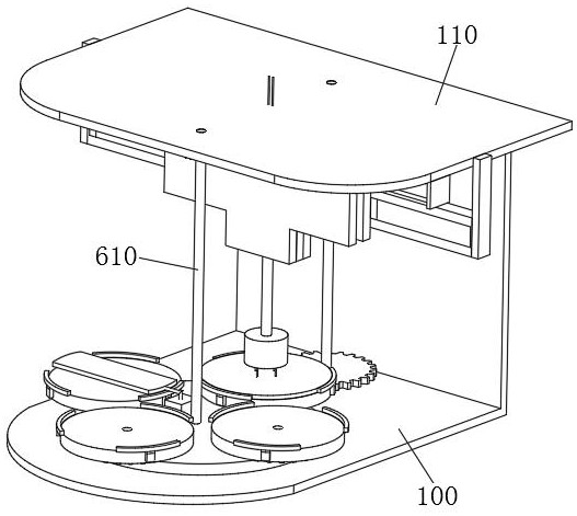
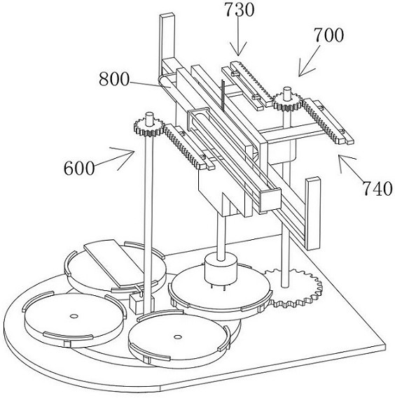
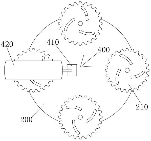
[0032] see Figure 1-11 As shown, a kind of semiconductor testing equipment comprises L-shaped bottom plate 100, the top of described L-shaped bottom plate 100 is fixedly connected with top plate 110, and the top surface of described L-shaped bottom plate 100 is rotatably connected with tray 200, and the top of described tray 200 The top surface of the tray 200 is fixedly connected with a dust suction mechanism 400 at the top of the top of the rotating shaft, and the bottom of the...
PUM
 Abstract
Description
Claims
Application Information