Wafer level chip size packaging structure and manufacturing method thereof

A wafer-level chip and size packaging technology, which is applied in semiconductor/solid-state device manufacturing, semiconductor/solid-state device components, semiconductor devices, etc., to achieve the effect of improving reliability and optimal bonding strength

Pending Publication Date: 2021-11-19
CHIPMOS TECH INC
View PDF6 Cites 0 Cited by
  • Summary
  • Abstract
  • Description
  • Claims
  • Application Information

AI Technical Summary

Problems solved by technology

[0004] The present invention is directed to a wafer-level chip size packaging structure and a manufacturing method thereof, which can reduce the occurrence of adverse effects on the wafer-level chip size packaging structure, thereby improving the reliability of the wafer-level chip size packaging structure

Method used


Image

  • Wafer level chip size packaging structure and manufacturing method thereof
  • Wafer level chip size packaging structure and manufacturing method thereof
  • Wafer level chip size packaging structure and manufacturing method thereof

Examples


Embodiment Construction

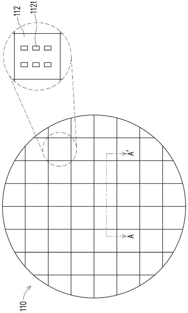
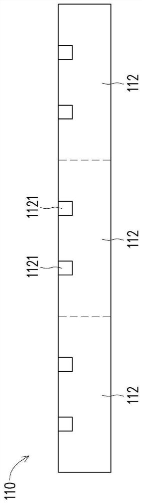
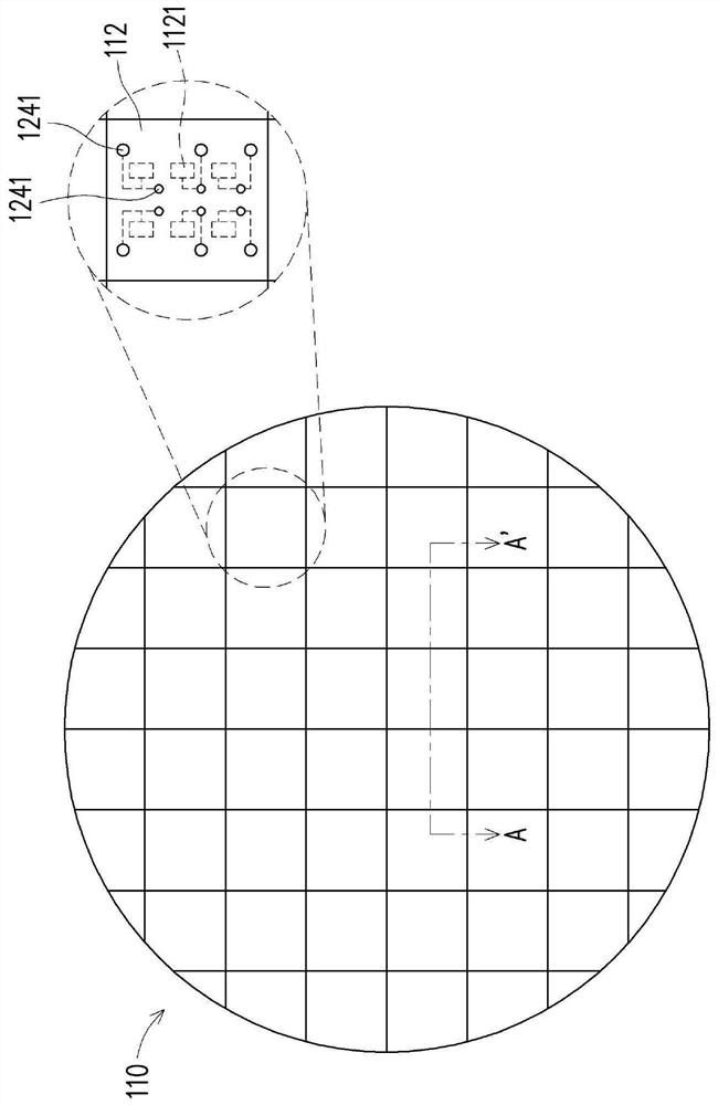
[0035] Reference will now be made in detail to the exemplary embodiments of the present invention, examples of which are illustrated in the accompanying drawings. Wherever possible, the same reference numbers will be used in the drawings and description to refer to the same or like parts.

[0036] Directional terms (eg, up, down, right, left, front, back, top, bottom) as used herein are used only as a reference to a drawn figure and are not intended to imply absolute orientation.

[0037] Any method described herein is in no way intended to be construed as requiring performance of its steps in a particular order, unless expressly stated otherwise.

[0038] The present invention will be described more fully below with reference to the accompanying drawings of this embodiment. However, the present invention can also be embodied in various forms and should not be limited to the embodiments described herein. The same or similar symbols represent the same or similar components, a...


PUM


Abstract

The invention provides a wafer level chip size packaging structure and a manufacturing method thereof. The wafer level chip size packaging structure comprises a first chip, a redistribution circuit layer, a plurality of ball bottom metal layers, a plurality of conductive columns, a second chip, packaging colloid and a plurality of connecting parts. The redistribution circuit layer is disposed on the first chip and electrically connected to pads thereof. The ball bottom metal layers are on the redistribution circuit layer. The conductive columns are located on a part of the ball bottom metal layers. The second chip is located on the other part of the ball bottom metal layers. The second chip has an active surface facing the plurality of ball bottom metal layers. The conductive columns surround the second chip. The packaging colloid at least packages the second chip and part of the side walls of the conductive columns. The top surface of the packaging colloid is lower than the top surfaces of the conductive columns. The connecting parts are located on the conductive columns and are electrically connected with the redistribution circuit layer through the conductive columns and the ball bottom metal layers. The connecting parts extend to the top surface of the packaging colloid.

Description

technical field [0001] The invention relates to a packaging structure and a manufacturing method thereof, in particular to a wafer-level chip size packaging structure and a manufacturing method thereof. Background technique [0002] Wafer level packaging technology (Wafer Level Packaging) is a packaging technology that performs chip size on the entire wafer, that is, most of the packaging work is completed at the wafer stage. Therefore, wafer level chip size packaging can reduce packaging Body size, and also quite advantageous in terms of process and material cost. [0003] Generally speaking, there are many factors affecting the reliability of WLCSP. For example, if the components on the wafer have poor bonding strength or are damaged during the process, it will have a bad impact on the WLCSP, thereby reducing the reliability of the WLCSP. Therefore, how to reduce the occurrence of adverse effects on the WLCSP, thereby improving the reliability of the WLCSP, has become a ...

Claims


Application Information

Patent Timeline
Patent Type & Authority Applications(China)
IPC IPC(8): H01L23/31H01L21/60H01L21/78
CPCH01L23/3114H01L24/26H01L24/83H01L21/78H01L2224/26H01L2224/83
Inventor 林俊辰
Owner CHIPMOS TECH INC
Why Eureka
Try Eureka