Display device and preparation method thereof

A technology of display device and display screen, applied in recognition devices, instruments, character and pattern recognition, etc., can solve the problems of reducing the efficiency of fingerprint recognition, weakening the light signal strength of the sensor chip under the screen, etc., so as to improve the efficiency of fingerprint recognition and enhance the light The effect of signal strength

Pending Publication Date: 2021-12-10
NANTONG FUJITSU MICROELECTRONICS
View PDF0 Cites 0 Cited by
  • Summary
  • Abstract
  • Description
  • Claims
  • Application Information

AI Technical Summary

Problems solved by technology

However, in the prior art, wire bonding (WB, Wire Bond) is usually required to connect the sensor chip and the circuit board in the fingerprint identification module, and WB will generate arc height. The arc height generated by WB leaves room for accommodation
But this will cause a gap between the sensor chip and the OLED screen, which will weaken the light signal strength received by the sensor chip under the screen and reduce the efficiency of fingerprint recognition.

Method used


Image

  • Display device and preparation method thereof
  • Display device and preparation method thereof
  • Display device and preparation method thereof

Examples


Embodiment Construction

[0040] The following will clearly and completely describe the technical solutions in the embodiments of the application with reference to the drawings in the embodiments of the application. Apparently, the described embodiments are only part of the embodiments of the application, not all of them. Based on the implementation manners in this application, all other implementation manners obtained by persons of ordinary skill in the art without making creative efforts belong to the scope of protection of this application.

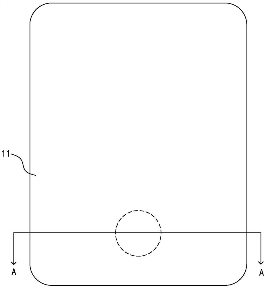
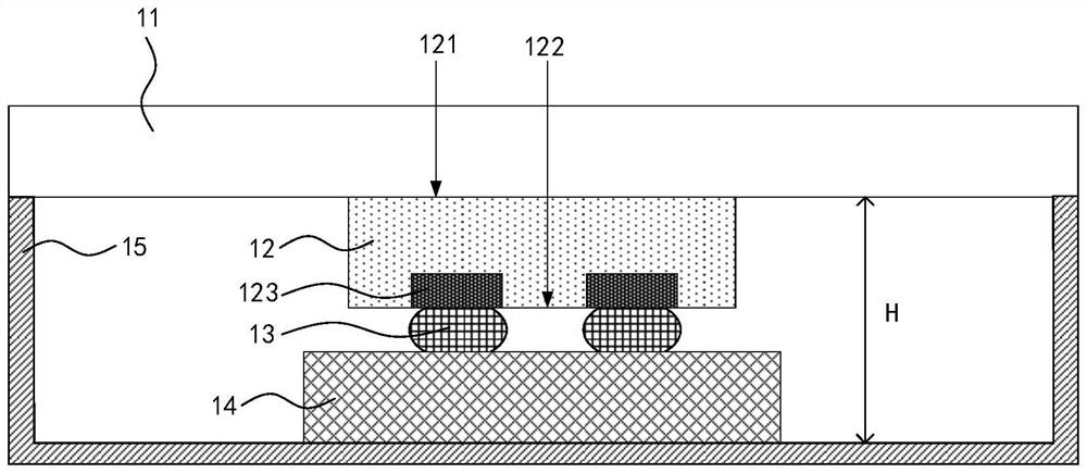
[0041] see figure 1 ,and figure 2 , figure 1 It is a schematic structural diagram of an embodiment of a display device of the present application, figure 2 for figure 1 A schematic cross-sectional view in the direction of A-A, the display device includes a display screen 11 , a sensor chip 12 , a conductive connector 13 and a circuit board 14 . figure 1 The sensor chip 12, the conductive connector 13 and the circuit board 14 are all located under the disp...


PUM


Abstract

The invention discloses a display device and a preparation method thereof, and belongs to the technical field of display. The display device comprises a display screen, a sensor chip, a conductive connecting piece and a circuit board. The sensor chip is arranged on one side of a non-display surface of the display screen, the sensor chip is provided with a front surface and a back surface which are oppositely arranged, the front surface faces the display screen and is used for receiving light rays penetrating through the display screen, and the back surface is provided with a bonding pad. The conductive connecting piece is arranged on the back surface of the sensor chip and is electrically connected with the bonding pad. The circuit board is arranged on the side, away from the sensor chip, of the conductive connecting piece, and the conductive connecting piece is electrically connected with the electric connecting points on the circuit board, so that when the circuit board drives the sensor chip to work, the sensor chip can conduct fingerprint recognition according to light rays. In the display device provided by the invention, the front surface of the sensor chip can be directly attached to the display screen without reserving a routing space, so that the intensity of an optical signal received by the sensor chip under the screen can be enhanced, and the fingerprint identification efficiency is improved.

Description

technical field [0001] The present application relates to the field of display technology, in particular to a display device and a manufacturing method thereof. Background technique [0002] With the development of display technology, the penetration rate of smart terminals such as mobile phones and tablets with OLED display panels is getting higher and higher. The mainstream off-screen fingerprint recognition technology is optical fingerprint recognition technology, that is, the fingerprint recognition module is transferred under the OLED screen. When fingerprint recognition is performed, some pixels emit light on the surface of the finger and are reflected to the fingerprint recognition module to perform fingerprint recognition. However, in the prior art, wire bonding (WB, Wire Bond) is usually required to connect the sensor chip and the circuit board in the fingerprint identification module, and WB will generate arc height. The arc height generated by WB leaves room for ...

Claims


Application Information

Patent Timeline
Patent Type & Authority Applications(China)
IPC IPC(8): G06K9/00G09F9/33H01L27/32
CPCG09F9/33H10K59/60
Inventor 梅枫谢文奇
Owner NANTONG FUJITSU MICROELECTRONICS
Why Eureka
Try Eureka