Unlock instant, AI-driven research and patent intelligence for your innovation.

Wafer defect detection method

A defect detection and wafer technology, applied in image data processing, instruments, calculations, etc., can solve the problems of missed detection, wrong detection, low efficiency, etc., and achieve the effect of improving the detection rate and reducing costs

Pending Publication Date: 2021-12-17
JIANGSU BRMICO ELECTRONICS
View PDF0 Cites 4 Cited by
  • Summary
  • Abstract
  • Description
  • Claims
  • Application Information

AI Technical Summary

Problems solved by technology

[0003] In order to solve the problem that manual screening of wafers with surface defects has low efficiency and is likely to cause missed and wrong detections, the present invention adopts the following technical solutions:

Method used


Image

  • Wafer defect detection method
  • Wafer defect detection method
  • Wafer defect detection method

Examples


Embodiment Construction

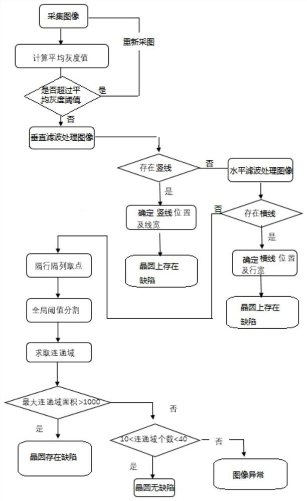
[0054] Combine below Figure 1 to Figure 3 The present invention will be further described.

[0055] A wafer defect detection method, comprising the steps of:

[0056] Step S1: Place the wafer on the imaging detector, press the surface of the wafer with a silicone prosthetic finger with a 45-degree twill pattern, and the imaging detector acquires an image after pressing. In order to detect defects on the wafer, since the defect of the wafer is usually at least one horizontal or vertical line appearing on the surface of the wafer, the 45-degree diagonal pattern can effectively distinguish the defects of the horizontal line and the vertical line on the wafer. Image processing is performed on the acquired image, and whether there is a defect on the image is judged. The process of image processing and judging is as follows: calculate the average gray level meanGray of the image, if the meanGray is not between 40 and 220, it means that the image acquisition is abnormal, and re-ac...


PUM


Abstract

The invention discloses a wafer defect detection method, and relates to the field of wafer testing. The method comprises the following steps: S1, acquiring an image of a wafer, performing image processing on the image to obtain an average gray value, and if the average gray value falls into an average gray value threshold interval range, entering S2; otherwise, collecting the wafer image again, and repeating S1; S2, performing vertical filtering processing on the image by adopting a RowMask convolution kernel, if the position of the vertical line defect is not found, entering S3, and otherwise, determining the position and width of the vertical line defect; S3, performing horizontal filtering processing on the image by adopting a HorMask convolution kernel, if the position of the transverse line defect is not found, entering S4, and otherwise, determining the position and width of the transverse line defect; and S4, carrying out background processing on the image, judging whether the background is abnormal or not, if the background is not abnormal, determining that the wafer is normal, otherwise, returning that the image is abnormal. Based on the method, the defects of the wafer can be adaptively screened, the labor cost is reduced, and the detection rate of the wafer defects is improved.

Description

technical field [0001] The invention relates to the field of wafer testing, in particular to a wafer defect detection method. Background technique [0002] After the wafer is diced, there may be internal damage. For example, there are problems such as defects, breakage or unpredictable damage, so the particles need to be screened before they can be sent to the packaging factory for packaging, otherwise the cost of manufacturing will be greatly increased. The deletion and selection of wafer particles is currently mainly through manual screening of surface defects to determine whether there are obvious traces on the surface of the particles, such as vertical lines, horizontal lines or other defects. However, the volume of the wafer is small, and the efficiency of manual screening is low, and it is easy to cause problems of missed detection and false detection. Contents of the invention [0003] In order to solve the problem that manual screening of wafers with surface defe...

Claims


Application Information

Patent Timeline
Patent Type & Authority Applications(China)
IPC IPC(8): G06T7/00G06T7/11G06T7/136G06T7/187G06T5/30G06T3/40
CPCG06T7/0004G06T7/11G06T7/136G06T7/187G06T3/40G06T5/30G06T2207/30108
Inventor 张莉王露刘磊
Owner JIANGSU BRMICO ELECTRONICS