Check patentability & draft patents in minutes with Patsnap Eureka AI!

Pixel circuit and display panel

A pixel circuit and electrical connection technology, applied in the direction of circuits, electrical components, static indicators, etc., can solve the problems of large area occupied by each pixel, the number of multi-signal lines used, and improve display resolution, so as to save wiring number, reducing leakage paths, and improving the effect of display resolution

Active Publication Date: 2021-12-17
WUHAN CHINA STAR OPTOELECTRONICS SEMICON DISPLAY TECH CO LTD
View PDF11 Cites 0 Cited by
  • Summary
  • Abstract
  • Description
  • Claims
  • Application Information

AI Technical Summary

Problems solved by technology

[0002] Most of each transistor in the pixel circuit of the traditional technical solution needs to configure at least one wiring as its control signal line and / or input signal line, which requires a large number of signal lines, resulting in an increasing area occupied by each pixel. The bigger it is, it is not conducive to improving the display resolution

Method used


Image

  • Pixel circuit and display panel
  • Pixel circuit and display panel
  • Pixel circuit and display panel

Examples


Embodiment Construction

[0032] The technical solutions in the embodiments of the present application will be clearly and completely described below in conjunction with the drawings in the embodiments of the present application. Apparently, the described embodiments are only some of the embodiments of this application, not all of them. Based on the embodiments in this application, all other embodiments obtained by those skilled in the art without making creative efforts belong to the scope of protection of this application.

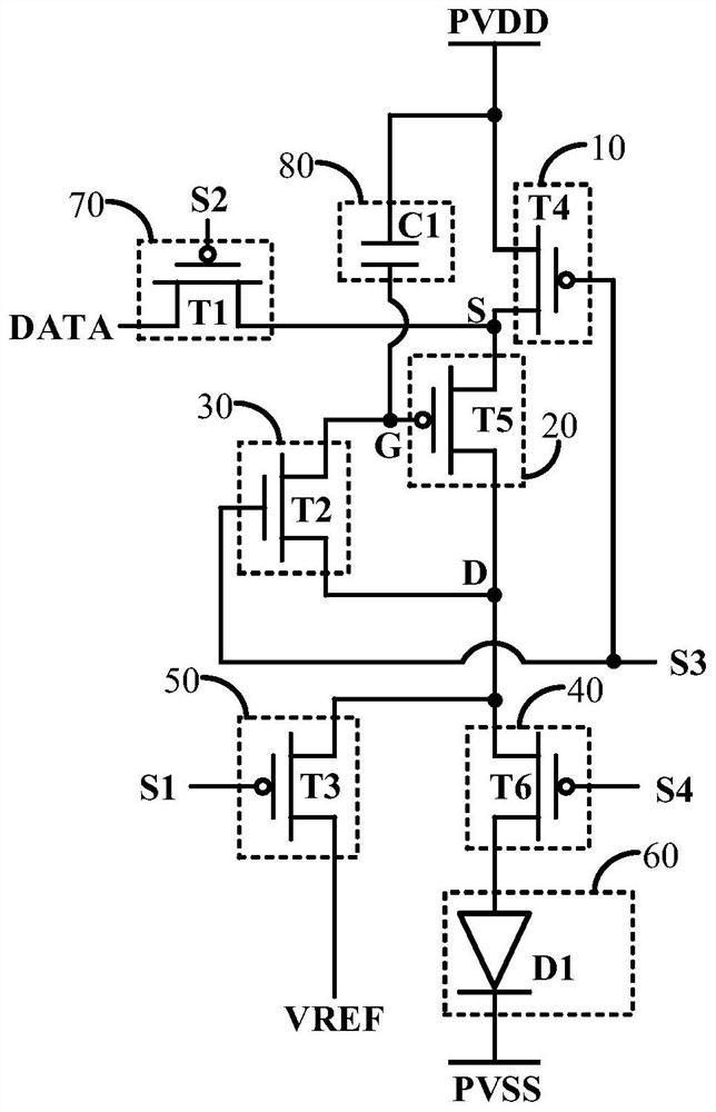
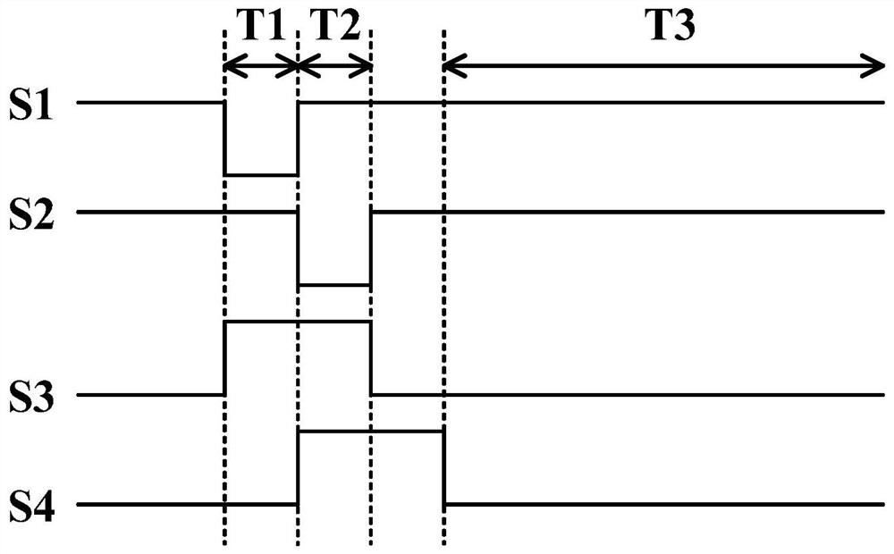
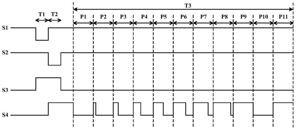
[0033] see Figure 1 to Figure 9 ,Such as figure 1 As shown, this embodiment provides a pixel circuit, which includes a second wiring, a first light emission control unit 10, a driving unit 20, and a compensation unit 30, and the control terminal of the first light emission control unit 10 is electrically connected to the second wiring One end of the driving unit 20 is electrically connected to one end of the first lighting control unit 10; one end of the compensation unit 30 i...


PUM


Abstract

The invention discloses a pixel circuit and a display panel, the pixel circuit comprises a second wiring, a first light-emitting control unit, a driving unit and a compensation unit, the control end of the first light-emitting control unit and the control end of the compensation unit share the second wiring, the number of the wiring of the pixel circuit can be reduced, and then the display resolution is improved; meanwhile, the control end of the driving unit is only provided with the compensation unit, so that the leakage path of the control end of the driving unit is reduced.

Description

technical field [0001] The present application relates to the field of display technology, in particular to a pixel circuit and a display panel. Background technique [0002] Most of each transistor in the pixel circuit of the traditional technical solution needs to configure at least one wiring as its control signal line and / or input signal line, which requires a large number of signal lines, resulting in an increasing area occupied by each pixel. The bigger it is, it is not conducive to improving the display resolution. [0003] It should be noted that the above introduction about the background technology is only for the purpose of clearly and completely understanding the technical solution of the present application. Therefore, it cannot be considered that the technical solutions mentioned above are known to those skilled in the art just because they appear in the background technology of the present application. Contents of the invention [0004] The present applica...

Claims


Application Information

Patent Timeline
IPC IPC(8): G09G3/3208G09G3/3233H01L27/15H01L27/32
CPCG09G3/3208G09G3/3233H01L27/156H10K59/131G09G2300/0819G09G2300/0861G09G2300/0842G09G2310/0251G09G3/2022G09G3/3225G09G2310/027G09G2340/0457
Inventor 王选芸陈诚戴超张毅先
Owner WUHAN CHINA STAR OPTOELECTRONICS SEMICON DISPLAY TECH CO LTD
Features
  • R&D
  • Intellectual Property
  • Life Sciences
  • Materials
  • Tech Scout
  • Unparalleled Data Quality
  • Higher Quality Content
  • 60% Fewer Hallucinations
Learn More