Power device with electrostatic protection structure and manufacturing method thereof

A power device, electrostatic protection technology, applied in semiconductor/solid-state device manufacturing, electrical components, semiconductor devices, etc., can solve the problems of power modules that cannot be minimized and difficult power modules

Inactive Publication Date: 2015-01-21
SHENZHEN KIA SEMICON TECH
View PDF4 Cites 3 Cited by
  • Summary
  • Abstract
  • Description
  • Claims
  • Application Information

AI Technical Summary

Problems solved by technology

The power device is a separate device. If it is necessary to carry out electrostatic protection, it is necessary to add a diode separately inside the package structure or build an electrostatic safety circuit on the control integrated

Method used


Image

  • Power device with electrostatic protection structure and manufacturing method thereof
  • Power device with electrostatic protection structure and manufacturing method thereof
  • Power device with electrostatic protection structure and manufacturing method thereof

Examples


Embodiment Construction

[0032] The present invention will be described in detail below in conjunction with the accompanying drawings and specific embodiments.

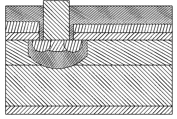
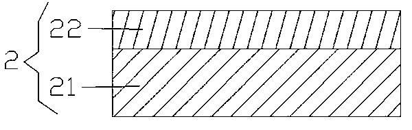
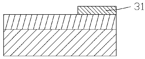
[0033] see Figure 15 The present invention provides a power device with an electrostatic protection structure, comprising: a drift layer 2, a drain region 5 formed under the drift layer 2, a drain electrode 6 formed under the drain region 5, and a drain electrode 6 formed under the drain region 5. The P-doped region 11 in the drift layer 2, the first N+ doped region 13 formed in the drift layer 2, the P+ doped region 14 formed in the drift layer 2, formed in the drift layer 2, the second insulating film 32 formed on the drift layer 2, the first P-doped region 11 and the first N+ doped region 14, formed on the first and second The polysilicon layer 33 on the insulating films 31, 32, the gate 34 formed on the second insulating film 32, the electrostatic protection layer 3 formed on the first insulating film 31, the gate 34 formed on the gate ...


PUM


Abstract

The invention discloses a power device with an electrostatic protection structure and a manufacturing method of the power device. The power device with the electrostatic protection structure comprises a drifting layer, a drain region, a drain electrode, a P- doped region, a first N+ doped region, a P+ doped region, a first insulating film, a second insulating film, a polycrystalline silicon layer, a gate electrode, an electrostatic protection layer, a third insulating film, a source electrode, an electrostatic electrode and a conductor layer. The electrostatic protection layer comprises a plurality of second P- doped regions and a plurality of second N+ doped regions, wherein the second P- doped regions and the second N+ doped regions are arranged alternately. By alternately arranging the P- doped regions and the second N+ doped regions in the power device, an electrostatic protection layer-Zener diode structure is formed, and thus space in a power module will not be occupied by an electrostatic protection circuit and the like while an electrostatic protection structure does not need to be additionally arranged, the space efficiency of the power module is improved, the number of wires and the number of some parasitic parameters are reduced, and the efficient power device is obtained.

Description

technical field [0001] The invention relates to the technical field of semiconductor devices, in particular to a power device with an electrostatic protection structure and a manufacturing method thereof. Background technique [0002] The substance whose conductivity is between a conductor and an insulator is a semiconductor. Electronic devices made of semiconductor materials are widely used in consumer electronics, computers and their peripherals, communications, power appliances, etc. because of their special conductive properties. field. A power device is an electronic device made of semiconductor materials, which is mainly used in circuits as power processing devices, such as figure 1 As shown in , it is a schematic structural diagram of an existing power device. [0003] Usually on an integrated circuit, a diode limiter (Diode Limiter) is used, and a bypass is used to discharge static electricity for electrostatic (ESD) protection. The power device is a separate devi...

Claims


Application Information

Patent Timeline
IPC IPC(8): H01L29/78H01L29/06H01L21/336
CPCH01L29/78H01L23/60H01L29/06H01L29/66477H01L29/866
Inventor 赵喜高
Owner SHENZHEN KIA SEMICON TECH
Why Eureka
Try Eureka