Lift-off method and laser machining apparatus

A technology of laser beams and optical devices, applied in laser welding equipment, metal processing equipment, manufacturing tools, etc., can solve problems such as longer processing time, inability to obtain processing results, damage, etc., and achieve the effect of suppressing quality degradation

Pending Publication Date: 2021-12-21
DISCO CORP
View PDF1 Cites 2 Cited by
  • Summary
  • Abstract
  • Description
  • Claims
  • Application Information

AI Technical Summary

Problems solved by technology

[0004] However, in the lift-off method of separating the composite substrate by irradiating a laser beam described in Patent Document 1, the composite substrate has warpage caused by bonding the optical device wafer to the transfer substrate or the like.
[0005] When such a composite substrate is irradiated with a laser beam, since the irradiation method (concentration state) of the laser beam is different between the outer peripheral part and the central part, there may be cases where only the outer peripheral part is peeled first and the central part is not peeled off or vice versa. The problem that the expected processing result cannot be obtained due to the phenomenon
[0006] Furthermore, when the entire composite substrate is additionally irradiated with a laser beam in order to promote the delamination of the non-delaminated region, there is a problem that not only the processing time becomes longer, but also the delaminated part is damaged and the quality deteriorates.

Method used


Image

  • Lift-off method and laser machining apparatus
  • Lift-off method and laser machining apparatus
  • Lift-off method and laser machining apparatus

Examples


no. 1 Embodiment approach 〕

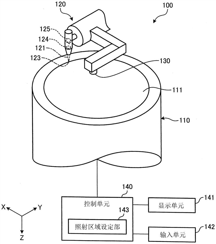
[0034] First, a laser processing apparatus according to a first embodiment of the present invention will be described. figure 1 It is a perspective view of main parts showing a configuration example of the laser processing apparatus according to the first embodiment. of the first embodiment figure 1 The laser processing device 100 shown is for figure 2 and image 3 The device for destroying the buffer layer 6 of the composite substrate 1 is shown.

[0035] (composite substrate)

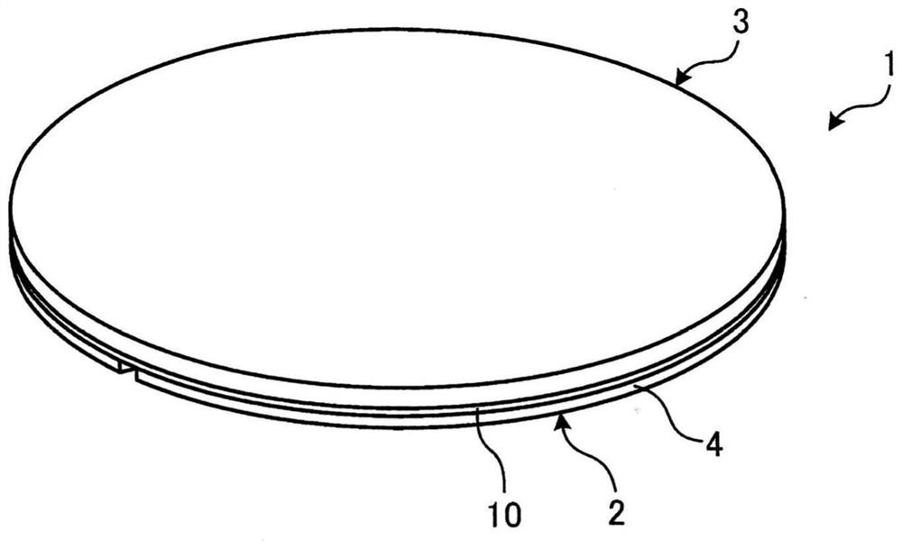
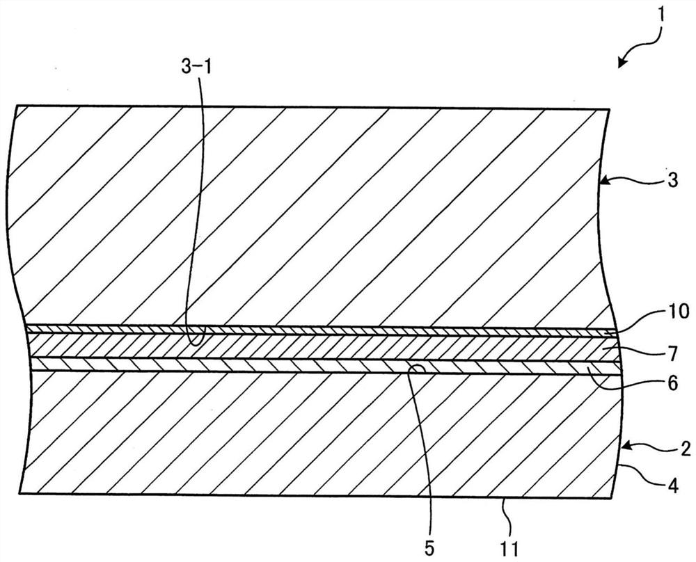
[0036] The composite substrate 1 will be described. figure 2 is shown as figure 1 A perspective view of a composite substrate to be processed by the laser processing apparatus shown. image 3 yes figure 2 A cross-sectional view of the main part of the composite substrate shown. Figure 4 is constituted figure 2 A perspective view of the opto-device wafer of the composite substrate shown. Figure 5 yes Figure 4 A cross-sectional view of the main part of the optical device wafer shown. ...

no. 2 Embodiment

[0085] A laser processing device and a lift-off method according to the second embodiment will be described. Figure 15 It is a plan view showing the annular region set by the irradiation region setting unit of the laser processing apparatus for carrying out the buffer layer breaking step of the lift-off method according to the second embodiment. In addition, in Figure 15 In the description, the same reference numerals are attached to the same parts as those in the first embodiment, and description thereof will be omitted.

[0086] The lift-off method of the second embodiment is the same as that of the first embodiment except that in the buffer layer destruction step 1002 , only the region irradiation step is performed instead of the whole irradiation step, and the irradiation conditions of the region irradiation step are different. In the second embodiment, in the buffer layer destroying step 1002, as processing content information, the area where the laser beam is irradiat...

no. 3 Embodiment approach 〕

[0095] A laser processing device and a lift-off method according to a third embodiment will be described. Figure 16 It is a plan view after the overall irradiation step of the buffer layer destruction step of the lift-off method according to the third embodiment. Figure 17 It is a plan view after the area irradiation step of the buffer layer destruction step of the lift-off method according to the third embodiment. In addition, in Figure 16 and Figure 17 In the description, the same reference numerals are attached to the same parts as those in the first embodiment, and description thereof will be omitted.

[0096] The lifting method of the third embodiment is the same as that of the first embodiment except that the irradiation conditions of the area irradiation step in the buffer layer destruction step 1002 are different. In the third embodiment, in the buffer layer destroying step 1002, as processing content information, information on the step of performing the overal...


PUM

PropertyMeasurementUnit
thicknessaaaaaaaaaa
thicknessaaaaaaaaaa
thicknessaaaaaaaaaa

Abstract

The invention provides a lift-off method and a laser processing apparatus which are capable of achieving desired processed results and preventing a reduction in the quality of processed products. A lift-off method includes a relocation substrate joining step of joining a relocation substrate to a surface of an optical device layer of an optical device wafer with a joining member interposed therebetween, thereby forming a composite substrate, a buffer layer breaking step of applying a pulsed laser beam having a wavelength transmittable through an epitaxy substrate and absorbable by a buffer layer to the buffer layer from a reverse side of the epitaxy substrate of the optical device wafer of the composite substrate, thereby breaking the buffer layer, and an optical device layer relocating step of peeling off the epitaxy substrate from the optical device layer, thereby relocating the optical device layer to the relocation substrate. In the buffer layer breaking step, irradiating conditions of the pulsed la-ser beam are changed for respective ring-shaped areas of the buffer layer, and the pulsed laser beam is applied to the optical device wafer under the changed irradiating conditions.

Description

technical field [0001] The present invention relates to a lift off method and a laser processing device. Background technique [0002] The following lift-off method is used: the optical device layer of the optical device wafer on which the optical device layer is laminated on the front surface of the epitaxial substrate with the buffer layer interposed is bonded to the transfer substrate with the bonding material, and the optical device wafer and the transfer substrate are bonded to the optical device wafer and the transfer substrate with The buffer layer of the composite substrate formed by bonding the bonding material is irradiated with a laser beam to destroy the buffer layer, and transfer the optical device layer from the epitaxial substrate to the transfer substrate (for example, refer to Patent Document 1). [0003] Patent Document 1: Japanese Patent Laid-Open No. 2013-229386 [0004] However, in the lift-off method of separating the composite substrate by irradiating...

Claims


Application Information

Patent Timeline
Patent Type & Authority Applications(China)
IPC IPC(8): B23K26/00B23K26/70
CPCB23K26/00B23K26/702H01L33/0095H01L33/005H01L21/7813H01L21/67092H01L33/12B23K26/20B23K26/0622B23K2103/56H01L33/007H01L33/0093
Inventor 小柳将三村纯也
Owner DISCO CORP
Why Eureka
Try Eureka