Wiring circuit board
A technology for wiring circuit substrates and grounding wires, which is applied in the field of wiring circuit substrates, can solve various problems and achieve the effect of efficient manufacturing
- Summary
- Abstract
- Description
- Claims
- Application Information
AI Technical Summary
Problems solved by technology
Method used
Image
Examples
no. 1 Embodiment approach >
[0043] 1. Wiring circuit board
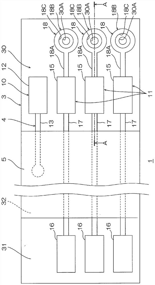
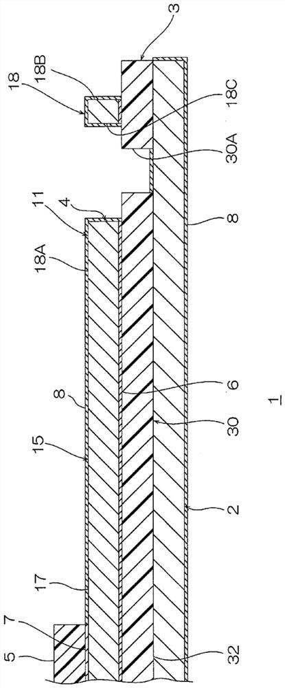
[0044] refer to figure 1 and figure 2 The wired circuit board 1 which is the first embodiment of the wired circuit board of the present invention will be described.
[0045] Such as figure 1 and figure 2 As shown, the wired circuit board 1 has a sheet shape having a thickness. The wired circuit board 1 has, for example, a rectangular shape in plan view. The wired circuit board 1 includes, for example, a flexible printed wiring board with a reinforcement layer having a metal support layer 2 as a reinforcement layer, a suspension board with circuit having a metal support layer 2 as a suspension (spring) layer, and the like.
[0046] Specifically, as figure 2 As shown, a wired circuit board 1 has a metal supporting layer 2 , an insulating base layer 3 as an example of an insulating layer, a seed film 6 , a conductor layer 4 , a first plating layer 7 , a cover insulating layer 5 , and a second plating layer 8 .
[0047] The metal support ...
no. 2 Embodiment approach >
[0108] Next, refer to Figure 6 , and a second embodiment of the wired circuit board of the present invention will be described. In addition, in 2nd Embodiment, the same code|symbol is attached|subjected to the same member as 1st Embodiment mentioned above, and the description is abbreviate|omitted.
[0109] In the first embodiment described above, if figure 2 As shown, the opening 18C communicates with the through-hole 30A, but the structure of the remaining portion of the ground wire is not limited thereto.
[0110] In the second embodiment, if Figure 6 and Figure 7 As shown, the ground wire stub portion 18 has a third stub portion 18D as an example of a conduction portion in addition to the first stub portion 18A and the second stub portion 18B.
[0111] The third residual portion 18D is disposed in the opening 18C, and fills the through hole 30A. Furthermore, the third remaining portion 18D is in contact with one surface in the thickness direction of the metal supp...
no. 3 Embodiment approach >
[0117] Next, refer to Figure 8 , and a third embodiment of the wired circuit board of the present invention will be described. In addition, in 3rd Embodiment, the same code|symbol is attached|subjected to the same member as 1st Embodiment mentioned above, and the description is abbreviate|omitted.
[0118] In the first embodiment described above, if figure 1 As shown, the remaining portion of the ground wire 18 is arranged on the opposite side to the connection wiring 17 with respect to the first terminal 15 , but the arrangement of the remaining portion of the ground wire is not limited to this. In particular, the remaining portion of the ground lead can be freely arranged without considering a reduction in the strength of the printed circuit board 1 , and therefore, can also be arranged in the inner portion of the printed circuit board 1 .
[0119] In the third embodiment, if Figure 8 As shown, the ground wire stub 18 is integrally formed with the connection wiring 17 ....
PUM
 Abstract
Description
Claims
Application Information
 - R&D
- Intellectual Property
- Life Sciences
- Materials
- Tech Scout
- Unparalleled Data Quality
- Higher Quality Content
- 60% Fewer Hallucinations
Browse by: Latest US Patents, China's latest patents, Technical Efficacy Thesaurus, Application Domain, Technology Topic, Popular Technical Reports.
© 2025 PatSnap. All rights reserved.Legal|Privacy policy|Modern Slavery Act Transparency Statement|Sitemap|About US| Contact US: help@patsnap.com


