Warpage control structure for metal base plate, semiconductor module, and inverter device
A metal base and metal plate technology, applied in semiconductor devices, semiconductor/solid-state device manufacturing, semiconductor/solid-state device components, etc.
- Summary
- Abstract
- Description
- Claims
- Application Information
AI Technical Summary
Problems solved by technology
Method used
Image
Examples
Embodiment Construction
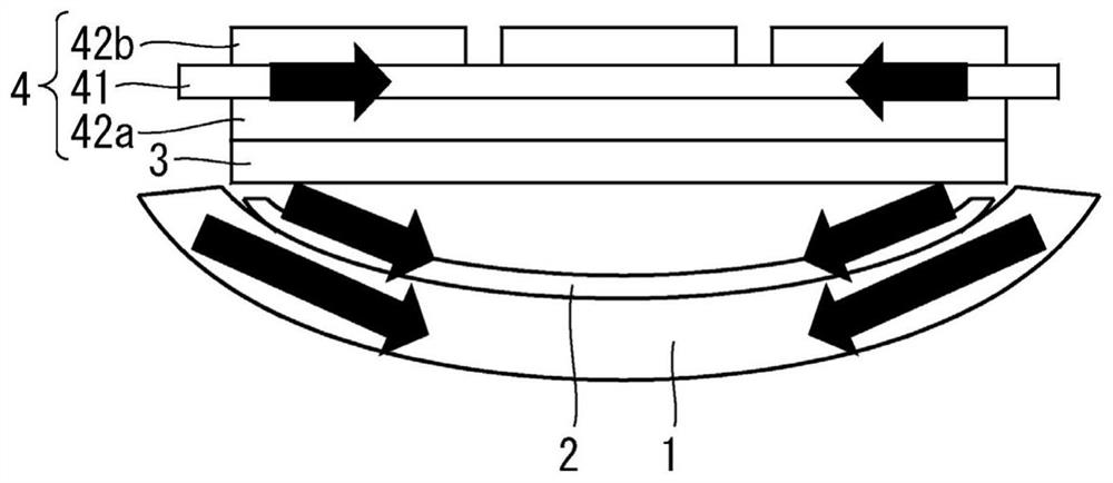
[0026] Embodiments of the present invention will be described below using the drawings. figure 1 It is a side view of the warpage control structure of the metal base plate which concerns on embodiment.
[0027] like figure 1 As shown, the warpage control structure of the metal base plate constitutes a part of the semiconductor module, and the warpage control structure of the metal base plate has a metal base plate 1 , a dissimilar metal layer 2 and an insulating substrate 4 .
[0028] The metal base plate 1 is approximately 100mm×100mm square in plan view, and has a thickness greater than or equal to 3.5mmt and less than or equal to 4.0mmt. In addition, as the material of the metal base plate 1, a material with high thermal conductivity such as aluminum, aluminum alloy, or copper is preferable. In this embodiment, aluminum is selected in order to reduce the total weight.
[0029] The dissimilar metal layer 2 is formed on the entire surface of the metal base plate 1 or only ...
PUM
 Abstract
Description
Claims
Application Information


