Electrostatic chuck, semiconductor etching equipment and wafer mounting method

An electrostatic chuck and semiconductor technology, applied in semiconductor/solid-state device manufacturing, circuits, electrical components, etc., can solve problems such as easy to block through holes, reduce the service life of electrostatic chucks, and affect the normal operation of mold ejector pins. Simple, life-extending effect

Pending Publication Date: 2022-01-18
INST OF MICROELECTRONICS CHINESE ACAD OF SCI +1
View PDF0 Cites 0 Cited by
  • Summary
  • Abstract
  • Description
  • Claims
  • Application Information

AI Technical Summary

Problems solved by technology

However, in the process of processing the wafer, some particles are usually produced, and these particles are easy to block the through hole, affecting the normal operation of the ejector pin, thereby reducing the service life of the electrostatic chuck

Method used


Image

  • Electrostatic chuck, semiconductor etching equipment and wafer mounting method
  • Electrostatic chuck, semiconductor etching equipment and wafer mounting method
  • Electrostatic chuck, semiconductor etching equipment and wafer mounting method

Examples


Embodiment Construction

[0042] In order to make the purpose, technical solutions and advantages of the embodiments of the present invention clearer, the technical solutions in the embodiments of the present invention will be clearly and completely described below in conjunction with the drawings in the embodiments of the present invention. Obviously, the described embodiments It is only some embodiments of the present invention, but not all embodiments. Based on the embodiments of the present invention, all other embodiments obtained by persons of ordinary skill in the art without making creative efforts belong to the protection scope of the present invention.

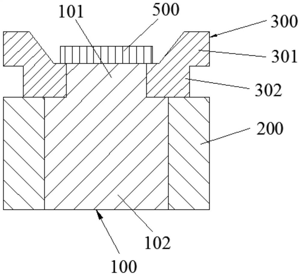
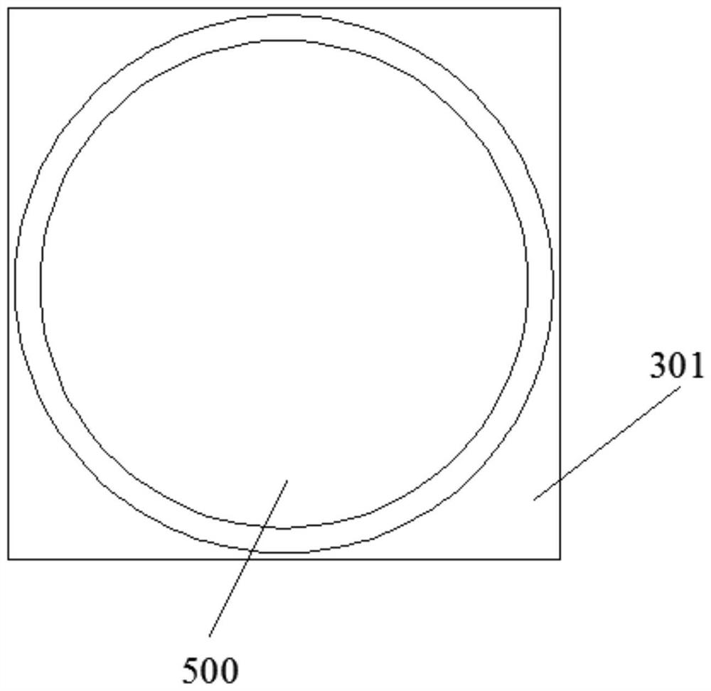
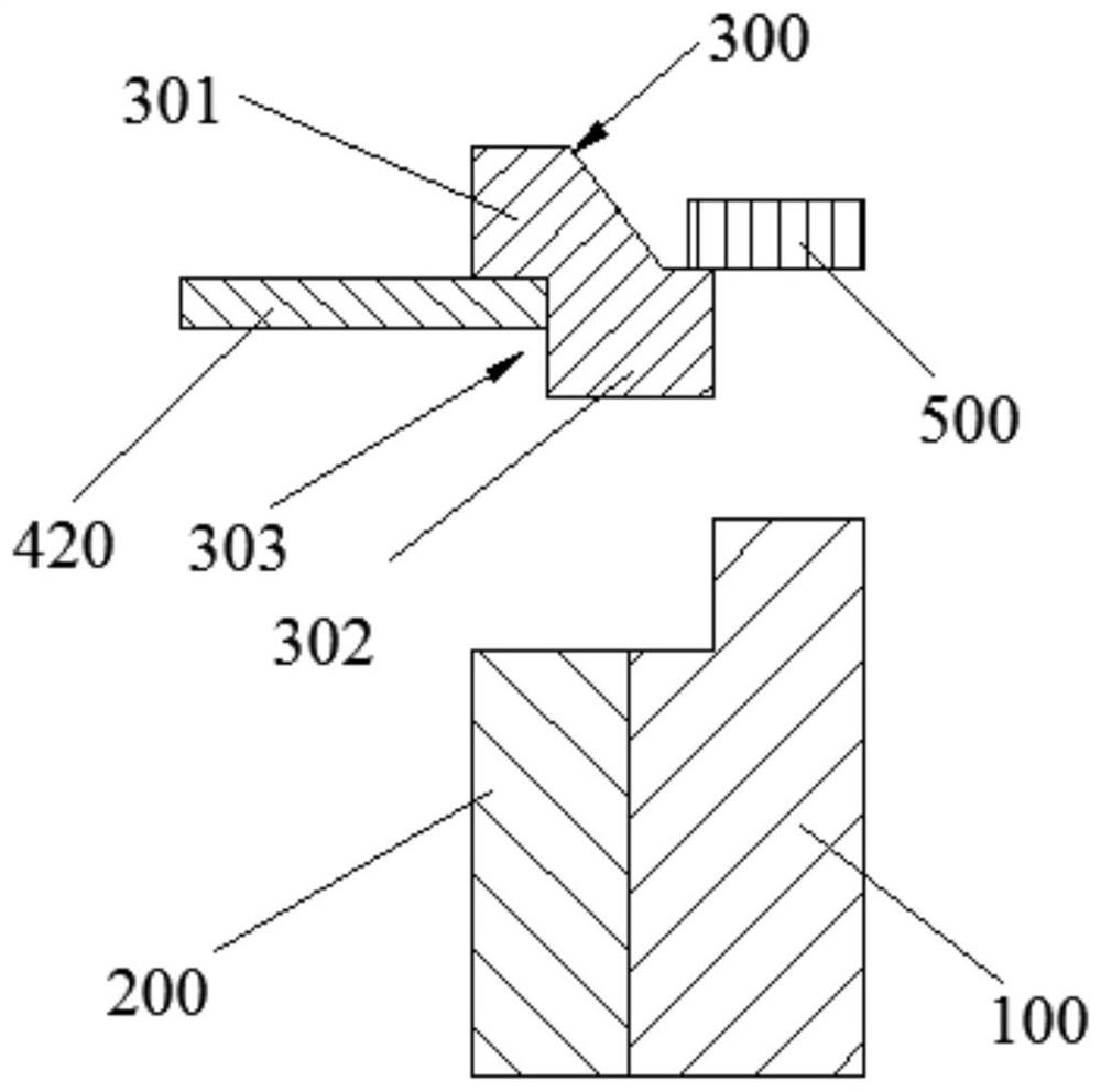
[0043] First aspect, combining figure 1 , the present invention provides an electrostatic chuck, comprising: a chuck body 100 , a base 200 and a limiting ring 300 . Wherein, the base 200 is used to support the chuck body 100 ; the limit ring 300 is used to support the wafer 500 .

[0044] The chuck body 100 includes: a chuck upper part 101 ...


PUM


Abstract

The invention provides an electrostatic chuck, semiconductor etching equipment and a wafer mounting method. The electrostatic chuck comprises a chuck body and a limiting ring; the limiting ring is used for supporting the wafer; a connecting part is arranged on the surface of the limiting ring and is used for driving the limiting ring and the wafer to move by being connected with a moving part, so that the wafer is mounted on the chuck body; and under the condition that the wafer is installed on the chuck body, the limiting ring is connected to the peripheral side of the chuck body in a sleeving mode. The service life of the electrostatic chuck can be prolonged.

Description

technical field [0001] The invention relates to the technical field of semiconductors, in particular to an electrostatic chuck, an etching semiconductor device and a method for installing a wafer. Background technique [0002] Electrostatic chucks are mainly used as mounting tables for fixing wafers in various processes of semiconductor device manufacturing. [0003] In addition to fixing the wafer, the electrostatic chuck is also used to remove the heat generated during the process from the wafer. For example, in order to improve the cooling effect of the wafer, the electrostatic chuck is arranged on the cooling device. Specifically, a backflow gas such as helium is used to flow into the back of the wafer to absorb heat from the wafer adsorbed on the chuck body. [0004] In order to install the wafer on the electrostatic chuck in the prior art, a through hole perpendicular to the upper surface of the chuck body is usually opened in the chuck body, and an ejector pin capabl...

Claims


Application Information

Patent Timeline
Patent Type & Authority Applications(China)
IPC IPC(8): H01L21/683H01L21/67
CPCH01L21/6833H01L21/67069
Inventor 金大镇李俊杰李琳王佳周娜
Owner INST OF MICROELECTRONICS CHINESE ACAD OF SCI
Why Eureka
Try Eureka