Unlock instant, AI-driven research and patent intelligence for your innovation.

Array substrate and display panel

A technology of array substrates and substrates, applied in instruments, nonlinear optics, optics, etc., can solve problems such as low penetration rate and low aperture ratio of pixel units, and achieve the goal of improving aperture ratio and penetration rate and improving penetration rate. Effect

Active Publication Date: 2022-01-28
TCL CHINA STAR OPTOELECTRONICS TECH CO LTD
View PDF7 Cites 0 Cited by
  • Summary
  • Abstract
  • Description
  • Claims
  • Application Information

AI Technical Summary

Problems solved by technology

[0005] The purpose of the present invention is to provide an array substrate and a display panel, which can solve the problems of low aperture ratio and low transmittance of pixel units existing in the prior art.

Method used


Image

  • Array substrate and display panel
  • Array substrate and display panel
  • Array substrate and display panel

Examples


Embodiment 1

[0050] This embodiment provides a display panel. The display panel includes an array substrate, a color filter substrate corresponding to the array substrate, and a liquid crystal layer arranged between the array substrate and the color filter substrate.

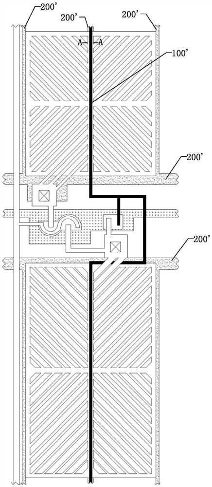
[0051] Such as image 3 As shown, the array substrate 100 includes: a substrate 101 and a plurality of pixel units 102 arrayed on the substrate 101 .

[0052] Wherein, the material of substrate 101 is one or more in glass, polyimide, polycarbonate, polyethylene terephthalate and polyethylene naphthalate, thus substrate 101 can have Good impact resistance can effectively protect the display panel.

[0053] Such as Figure 4 As shown, each pixel unit 102 is divided into a main pixel area 1021 and a sub-pixel area 1022 . Each pixel unit 102 includes: a scanning line 1, a first common line 2, a first sharing line 3, a data line 4, a main pixel electrode 5, a sub-pixel electrode 6, a main pixel TFT 7, a sub-pixel TFT 8. Shar...

Embodiment 2

[0071] Such as Figure 10-Figure 13 As shown, Embodiment 2 includes most of the technical features of Embodiment 1. The difference between Embodiment 2 and Embodiment 1 is that the second common line 10 of Embodiment 1 is removed in Embodiment 2, and the second common line 10 of Embodiment 1 is removed. A second sharing line 11 is set at the position of the two common lines 10 .

[0072] Such as Figure 10 , Figure 11 As shown, one end of the second sharing line 11 is electrically connected to the first sharing line 3, and the other end extends from the sub-pixel region 1022 of one pixel unit 102 to the adjacent one along the extending direction of the data line 4. The main pixel area 1021 of the pixel unit 102 . The second sharing line 11 is parallel to the data line and spaced apart from the data line 4 . Wherein, the second sharing line 11 is arranged on the same layer as the scanning line 1 , the first common line 2 and the first sharing line 3 .

[0073] Such as F...


PUM


Abstract

The invention relates to an array substrate and a display panel. A first common line and a first sharing line are arranged on the two sides of a scanning line respectively, so that the situation that the first sharing line longitudinally penetrates through a primary pixel area and a secondary pixel area in the prior art is avoided, and then the aperture opening ratio and the penetration rate of the array substrate are improved. The first common line, the first sharing line and the scanning line are arranged on the same layer, so that the penetration rate of the array substrate is further improved.

Description

technical field [0001] The present application relates to the field of display technology, in particular to an array substrate and a display panel. Background technique [0002] At present, in vertical alignment (English full name: Vertical Alignment, VA for short) liquid crystal display panels, under different viewing angles, the birefringence index of the liquid crystal molecules is quite different, and the color shift is serious. High Vertical Alignment (English full name: HighVertical Alignment, HVA for short) liquid crystal display panel needs to design multi-domain display to improve color shift. Based on the electrical principle, the pixel unit is divided into the main pixel (full name in English: main pixel) area and the sub-pixel (full name in English: sub pixel) area with different rotation angles of liquid crystal molecules. 8 domains are displayed. [0003] The current 8domain display is to control the main pixel electrode through a main pixel thin film transis...

Claims


Application Information

Patent Timeline
IPC IPC(8): G02F1/1362G02F1/1368
CPCG02F1/136286G02F1/1368G02F1/134345G02F1/133757G02F1/13624G02F1/13306G02F1/1362G02F1/134309
Inventor 肖军城李吉龙芬赵迎春葛茹
Owner TCL CHINA STAR OPTOELECTRONICS TECH CO LTD