Current source circuit
A technology of current source and power supply voltage, applied in the field of circuits, can solve problems such as instant start-up interference, and achieve the effect of reducing switching jitter
- Summary
- Abstract
- Description
- Claims
- Application Information
AI Technical Summary
Problems solved by technology
Method used
Image
Examples
Embodiment 1
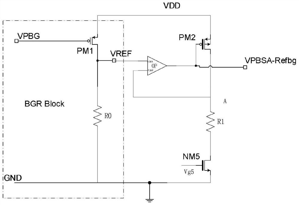
[0046] One embodiment of the present invention, a current source circuit, comprising:
[0047] A power supply voltage input circuit for inputting a power supply voltage;
[0048] The power supply voltage anti-shake circuit is connected with the power supply voltage input circuit; the power supply voltage anti-shake circuit includes:
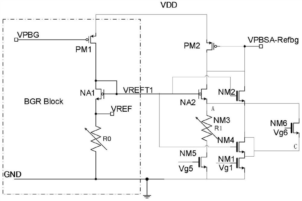
[0049] The first intrinsic NMOS transistor NA2, the first enhanced NMOS transistor NM1, the second enhanced NMOS transistor NM2, the third enhanced NMOS transistor NM4, the fourth enhanced NMOS transistor NM5, and the fifth enhanced NMOS transistor NM6.
[0050] The third enhanced NMOS transistor NM4 is connected to the first enhanced NMOS transistor NM1 and the second enhanced NMOS transistor NM2; the drain of the third enhanced NMOS transistor NM4 is connected to the third enhanced NMOS transistor NM4 The source of the transistor NM4 is connected; the third enhanced NMOS transistor NM4 is connected to the power supply voltage.
[0051] The so...
Embodiment 2
[0059] Based on the above embodiments, the current source circuit in this embodiment, such as figure 2 shown, also includes:
[0060] The first PMOS transistor PM2; the source of the first PMOS transistor PM2 is connected to the power supply voltage input circuit; the gate of the first PMOS transistor PM2 is connected to the drain of the second enhanced NMOS transistor NM2 Connect to the current output port of the current source.
[0061] The gate of the first intrinsic NMOS transistor NA2 is connected to the power supply voltage input circuit, the gate of the second enhanced NMOS transistor NM2, and the gate of the third enhanced NMOS transistor NM4; The drain of the first intrinsic NMOS transistor NA2 is connected to the drain of the first PMOS transistor PM2 and the drain of the second enhancement NMOS transistor NM2 .
[0062] The drain of the first enhanced NMOS transistor NM1 is connected to the source of the third enhanced NMOS transistor NM4; the source of the first...
Embodiment 3
[0073] Based on the above-mentioned embodiment, in the current source circuit in this embodiment, as figure 2 As shown, the power supply voltage input circuit includes:
[0074] The second PMOS transistor PM1, the second intrinsic NMOS transistor NA1, and the second resistor R0.
[0075] The source of the second PMOS transistor PM1 is connected to the source of the first PMOS transistor PM2; the drain of the second PMOS transistor PM1 is connected to the drain of the second intrinsic NMOS transistor NA1.
[0076] The drain of the second intrinsic NMOS transistor NA1 is also connected to the gate of the second intrinsic NMOS transistor NA1; the source of the second intrinsic NMOS transistor NA1 is connected to a port for inputting a reference voltage; The gate of the second intrinsic NMOS transistor NA1 is connected to the gate of the first intrinsic NMOS transistor NA2; the source of the second intrinsic NMOS transistor NA1 is also connected to the gate of the second resisto...
PUM
 Abstract
Description
Claims
Application Information
 - R&D Engineer
- R&D Manager
- IP Professional
- Industry Leading Data Capabilities
- Powerful AI technology
- Patent DNA Extraction
Browse by: Latest US Patents, China's latest patents, Technical Efficacy Thesaurus, Application Domain, Technology Topic, Popular Technical Reports.
© 2024 PatSnap. All rights reserved.Legal|Privacy policy|Modern Slavery Act Transparency Statement|Sitemap|About US| Contact US: help@patsnap.com


