Packaging method and packaging equipment for PCBA (Printed Circuit Board Assembly)
A packaging method and technology in the horizontal direction, applied in the secondary processing of printed circuits, electrical components, printed circuit manufacturing, etc., can solve the problems of high design and production costs, high costs, inability to achieve waterproof and shockproof, and achieve fast curing efficiency. , the effect of high production efficiency
- Summary
- Abstract
- Description
- Claims
- Application Information
AI Technical Summary
Problems solved by technology
Method used
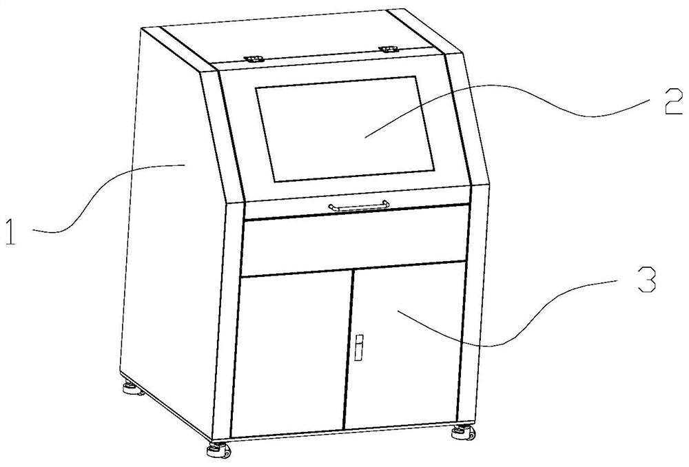
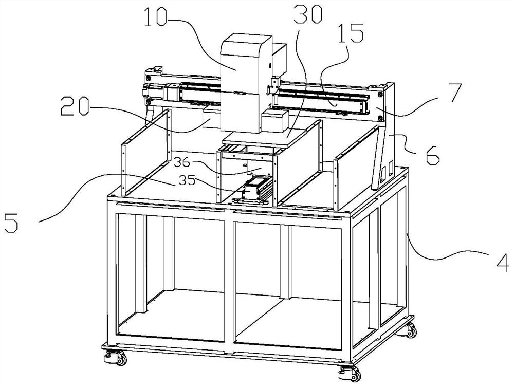
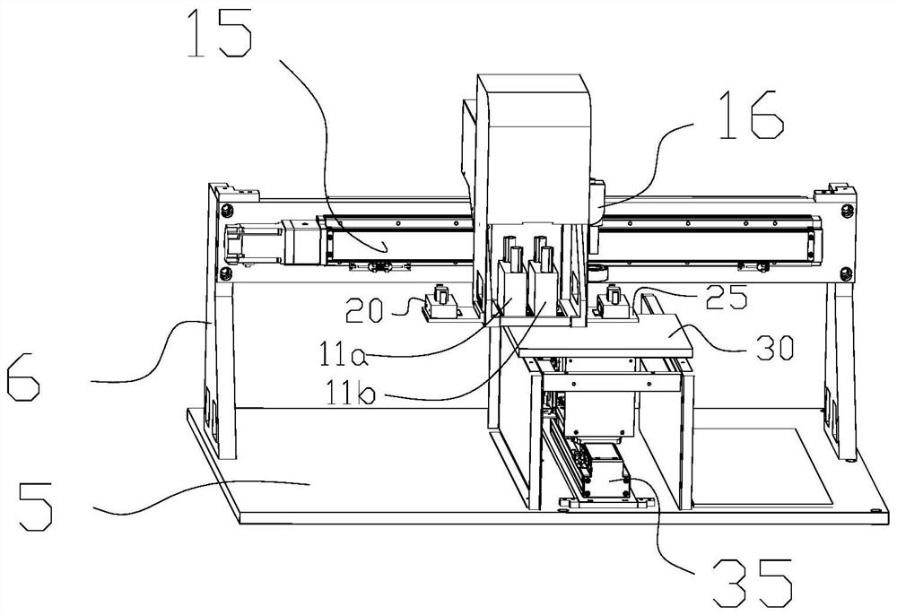
Image

Examples
Embodiment Construction
[0124] In order to enable those skilled in the art to better understand the technical solutions in the present disclosure, the technical solutions in the embodiments of the present disclosure will be clearly and completely described below in conjunction with the drawings in the embodiments of the present disclosure. Obviously, the described The embodiments are only some of the embodiments of the present disclosure, not all of them. Based on the embodiments in the present disclosure, all other embodiments obtained by persons of ordinary skill in the art without creative efforts shall fall within the protection scope of the present disclosure.
[0125] It should be noted that when an element is referred to as being “disposed on” another element, it may be directly on the other element or there may be another element in between. When an element is referred to as being "connected to" another element, it can be directly connected to the other element or it may be present intervenin...
PUM
 Abstract
Description
Claims
Application Information
 - R&D
- Intellectual Property
- Life Sciences
- Materials
- Tech Scout
- Unparalleled Data Quality
- Higher Quality Content
- 60% Fewer Hallucinations
Browse by: Latest US Patents, China's latest patents, Technical Efficacy Thesaurus, Application Domain, Technology Topic, Popular Technical Reports.
© 2025 PatSnap. All rights reserved.Legal|Privacy policy|Modern Slavery Act Transparency Statement|Sitemap|About US| Contact US: help@patsnap.com