A wafer level packaging structure of a filter and a process thereof

A wafer-level packaging and filter technology, applied in electrical components, impedance networks, etc., can solve the problems of strict flatness requirements of substrates and sealing covers, inconsistent performance of accurate devices, and high cost of surface sealing covers. Process yield, small warpage, and the effect of reducing difficulty

Pending Publication Date: 2019-05-07
XIAMEN SKY SEMICON TECH CO LTD
View PDF0 Cites 12 Cited by
  • Summary
  • Abstract
  • Description
  • Claims
  • Application Information

AI Technical Summary

Problems solved by technology

[0005] 1. The cost of the surface sealing cover is relatively high;
[0006] 2. The reliability of the product has strict requirements on the flatness of the substrate and the sealing cover, which is easy to cause failure
[0007] 3. A series of uncertainties such as the accuracy of device installation, the influence of signal guides, and the angle of welding will cause inconsistency in device performance and even damage the filter

Method used


Image

  • A wafer level packaging structure of a filter and a process thereof
  • A wafer level packaging structure of a filter and a process thereof
  • A wafer level packaging structure of a filter and a process thereof

Examples


Embodiment 1

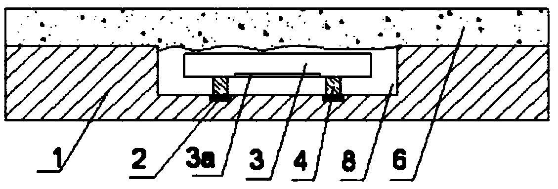
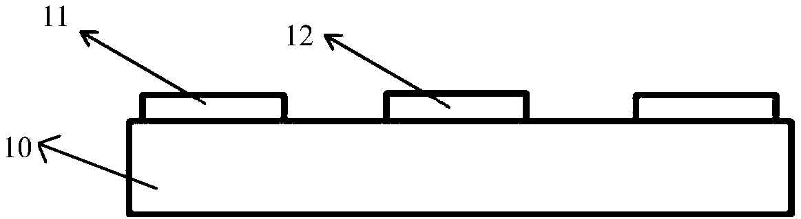
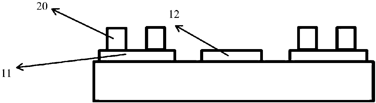
[0039] refer to Image 6 , a filter wafer-level packaging structure of the present invention, which is a thin-film packaging structure, including a chip substrate 10, a first thin-film layer 20, a second thin-film layer 30, and metal connectors 40 and the like. see figure 2 The working surface of the chip substrate 10 is provided with pads 11 and IDT 12, the positions of the pads 11 and IDT12 are not limited, and can be designed according to requirements. For example: for a single chip, its IDT (interdigital transducer) is positioned at the central position of chip substrate 10, and bonding pad 11 is positioned at chip substrate 10 edges, and is spaced certain distance between bonding pad 11 and IDT12, and bonding pad 11 quantity is different Unique, can be two or even more. The chip of the present invention is a surface acoustic wave filter, or other filters with similar functions.

[0040] The first thin film layer 20 is coated on the working surface of the chip substrat...

Embodiment 2

[0052] see Figure 7 , a filter wafer-level packaging structure and its process, its main structure and process are generally the same as in the first embodiment, the difference is that: the metal connector 40 is a hollow connector, and the metal connector 40 is covered Related steps of filling the layer 41 , the filling layer 41 plays a role of protecting the metal connector 40 . The upper surface of the metal connector 40 can be extended according to the welding position, and nickel-palladium-gold, nickel-gold, titanium-copper pads, etc. can be made at any position to form the welding part 40 .


PUM


Abstract

The invention discloses a wafer-level packaging structure of a filter and a process thereof, and the structure comprises a chip substrate, and the working surface of the chip substrate is provided with a bonding pad and an IDT. The structure further comprises a first film layer, a second film layer and a metal connecting piece. Wherein the first thin film layer is located on the working surface ofthe chip substrate and exposes a part of the bonding pad and the IDT; The second thin film layer is positioned on the surface of the first thin film layer and exposes part of the bonding pad; A protection cavity is formed among the second thin film layer, the first thin film layer and the working surface of the chip substrate, and the IDT is located in the protection cavity; And the metal connecting piece is electrically connected with the bonding pad and is provided with a welding part. The surface of the filter is covered with the two films, the cavity is formed, the packaging reliability can be improved, the technological process is greatly optimized, and the whole packaging cost is low. Due to the fact that the thin film is adopted to serve as the cavity cover plate, smaller warpage is achieved after wafer level packaging, and the process yield of products is improved.

Description

technical field [0001] The invention relates to the field of semiconductor packaging, in particular to a wafer-level packaging structure of a filter and a process thereof. Background technique [0002] The surface acoustic wave filter uses the excitation, propagation and reception of the surface acoustic wave on the piezoelectric material to complete its filtering characteristics. The surface acoustic wave wavelength is in the range of 100 μm to 2 μm, and it is a mechanical wave that is very sensitive to its propagation surface. In order for the surface acoustic waves in an acoustic wave component to propagate without disturbance, there is a cavity above the surface of the chip in the package. [0003] At present, the main packaging technology of filters is ceramic, metal, plastic packaging and flip-chip packaging with lead bonding, such as figure 1 A surface acoustic wave filter packaging structure, which includes a substrate (1), a groove (8) is provided on the back of t...

Claims


Application Information

Patent Timeline
Patent Type & Authority Applications(China)
IPC IPC(8): H03H3/02
Inventor 姜峰
Owner XIAMEN SKY SEMICON TECH CO LTD
Why Eureka
Try Eureka