

Wafer-level chip size encapsulation technology for GaAs (gallium arsenide) CCD (Charge Coupled Device) image sensor
A technology of chip size packaging and image sensor, which is applied in the process of producing decorative surface effects, decorative art, metal material coating process, etc., can solve the problems of low reliability and interconnection density, high process cost, etc., and achieve reduction Packaging cost and process difficulty, increasing interconnection density, and the effect of reliable packaging
- Summary
- Abstract
- Description
- Claims
- Application Information
AI Technical Summary
Problems solved by technology
Method used
Image

Examples
Embodiment Construction
[0056] In order to fully demonstrate the advantages and positive effects of the present invention, the substantive features and remarkable progress of the present invention will be further described below in conjunction with the accompanying drawings and embodiments.
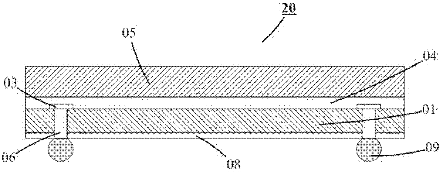
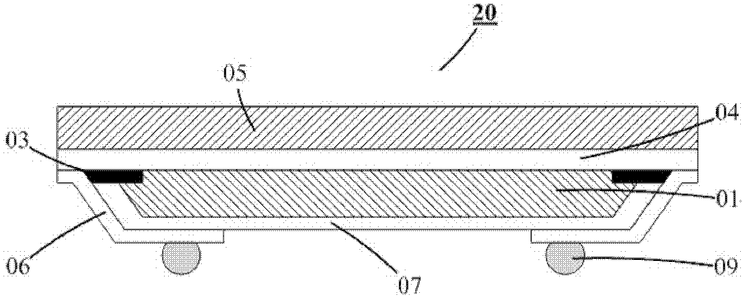
[0057] Such as image 3 Shown is a cross-sectional view of a GaAs CCD image sensor wafer-level chip-scale package 20 manufactured according to the best embodiment of the present invention.
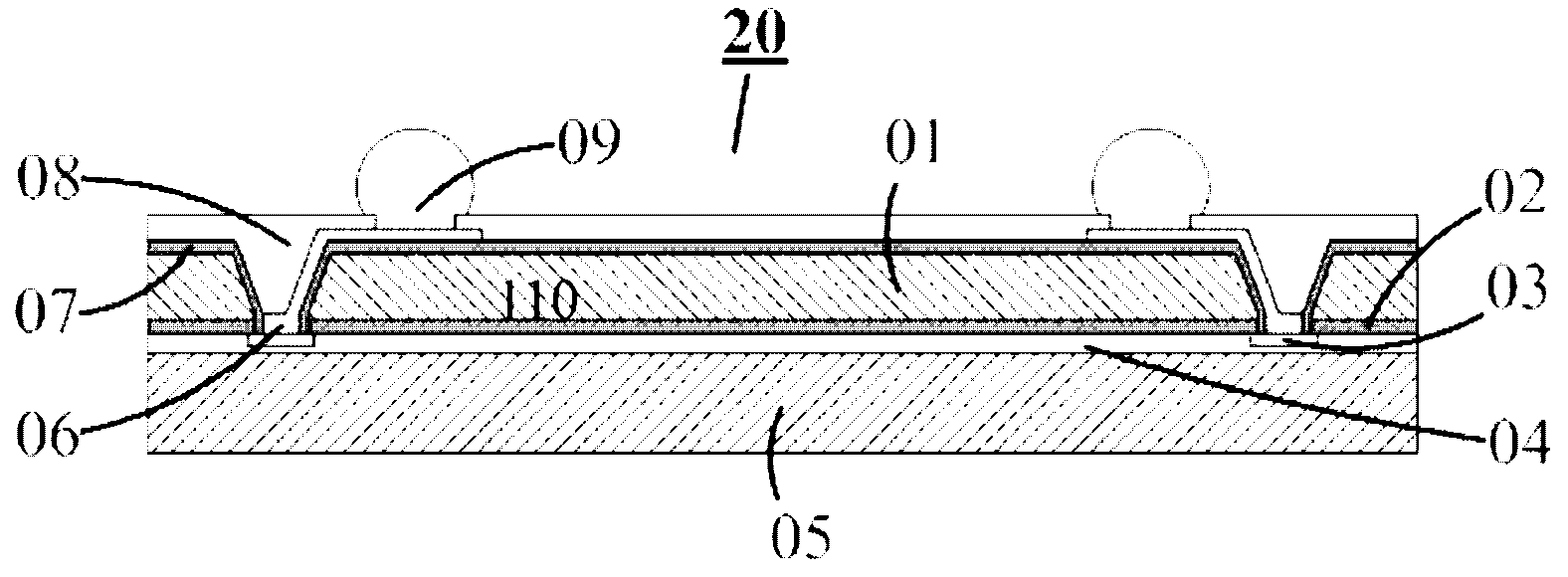
[0058] Such as Figure 4 Shown is a cross-sectional view of the packaging structure and interconnection structure according to the best implementation mode of the present invention. In this embodiment, the trapezoidal groove structure 13 includes a circle of vertical interconnection vias 14, and the bumps 09 adopt a partial array structure. . From Figure 4 It can be seen that the signal of the sensor chip is transmitted from the active surface to the back of the chip through the vertical interconnection hole and the trap...
PUM
| Property | Measurement | Unit |
|---|---|---|
| thickness | aaaaa | aaaaa |
Abstract
Description
Claims
Application Information