Radio frequency module three-dimensional stacking structure and manufacturing method thereof

A three-dimensional stacking, radio frequency module technology, applied in electrical components, electrical solid devices, circuits, etc., can solve problems such as no solution, difficult wafer bonding process multi-layer stacking, etc., to achieve excellent performance and solve process temperature. Compatibility, good structural strength effect

Active Publication Date: 2021-02-26
SOUTHWEST CHINA RES INST OF ELECTRONICS EQUIP
View PDF7 Cites 6 Cited by
  • Summary
  • Abstract
  • Description
  • Claims
  • Application Information

AI Technical Summary

Problems solved by technology

[0004] In the process of three-dimensional stacking of high-density substrates of various materials, due to the different shapes and sizes of substrates of different materials, it is difficult to perform multi-layer stacking through wafer bonding process , how to design the stacking structure and process to meet the high-density, high-performance, and high-reliability application requirements of electronic equipment systems, the existing technology has not yet given a solution

Method used


Image

  • Radio frequency module three-dimensional stacking structure and manufacturing method thereof
  • Radio frequency module three-dimensional stacking structure and manufacturing method thereof
  • Radio frequency module three-dimensional stacking structure and manufacturing method thereof

Examples


Embodiment Construction

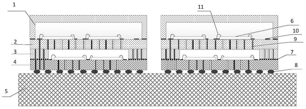
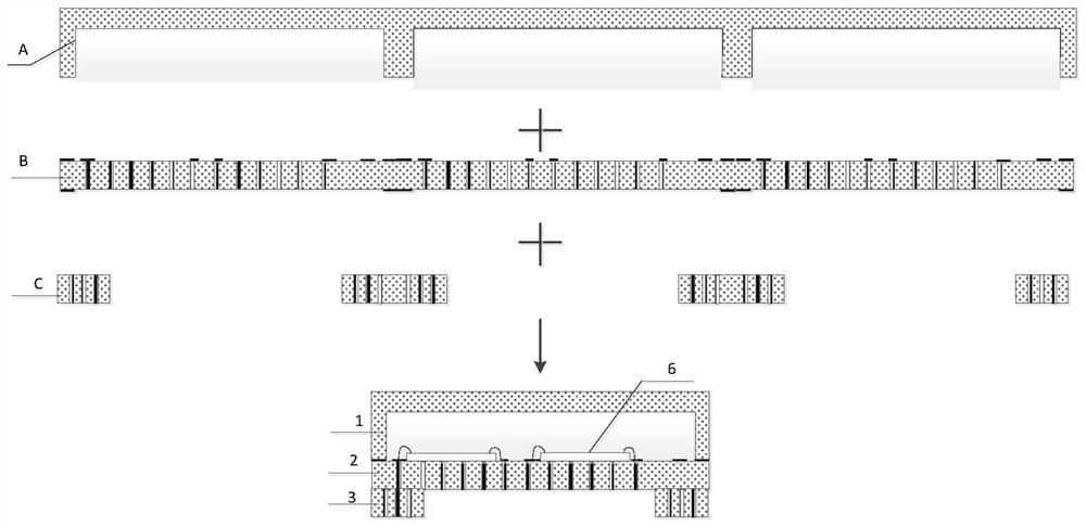
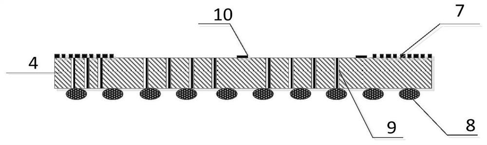
[0032] Such as Figure 1~6 As shown, a three-dimensional stacked structure of a radio frequency module includes a glass cap layer 1, a glass carrier layer 2, a glass interposer frame layer 3, a silicon-based carrier layer 4, a ceramic packaging layer 5 and a radio frequency chip 6; a glass carrier layer 2, a glass Both the transfer frame layer 3 and the silicon-based carrier layer 4 are provided with through holes 9 and interconnection lines 10; the glass cap layer 1, the glass carrier layer 2, the glass transfer frame layer 3, the silicon-based carrier layer 4, and the ceramic packaging layer 5 Stacked and interconnected sequentially from top to bottom; the radio frequency chip 6 is located on the upper surface of the silicon-based carrier layer 4 and the upper surface of the glass carrier layer 2, and is connected to the circuit pad on the carrier layer through a lead structure; the glass cap layer 1, the glass carrier The layer 2 and the glass transfer frame layer 3 form a ...


PUM

PropertyMeasurementUnit
thicknessaaaaaaaaaa
diameteraaaaaaaaaa
diameteraaaaaaaaaa

Abstract

The invention discloses a radio frequency module three-dimensional stacking structure and a manufacturing method thereof. The radio frequency module three-dimensional stacking structure comprises a glass cap layer, a glass carrier layer, a glass transfer frame layer, a silicon-based carrier layer, a ceramic packaging layer and radio frequency chips. The glass carrier layer, the glass transfer frame layer and the silicon-based carrier layer are all provided with through holes and interconnection lines; the glass cap layer, the glass carrier layer, the glass transfer frame layer, the silicon-based carrier layer and the ceramic packaging layer are stacked and interconnected in sequence from top to bottom; and the radio frequency chips are located on the upper surface of the silicon-based carrier layer and the upper surface of the glass carrier layer, and are connected with circuit bonding pads on the carrier layer through lead structures. Through combination and stacking of high-density substrates made of various materials, the radio frequency module is better in performance and higher in density, and the integration process is simple, flexible, better in reliability and the like.

Description

technical field [0001] The invention relates to the field of microelectronic integrated packaging, and more specifically, to a three-dimensional stacking structure of radio frequency modules and a manufacturing method thereof. Background technique [0002] In order to achieve the best performance in the RF module, a variety of chips with different materials and processes are used for heterogeneous integration. The traditional two-dimensional planar integrated multi-chip module packaging technology (MultiChipModule, MCM) has been difficult to meet the continuous miniaturization, light weight, and multi-functional development requirements of electronic equipment. It requires three-dimensional stacking in the vertical direction to meet the application requirements of radio frequency modules. . The RF microsystem integration technology disclosed in Chinese patents CN107359156B and CN207861877U uses silicon as the substrate material and utilizes through-silicon via (TSV) and waf...

Claims


Application Information

Patent Timeline
Patent Type & Authority Applications(China)
IPC IPC(8): H01L25/07H01L23/31H01L23/498H01L23/66
CPCH01L25/072H01L23/3121H01L23/49816H01L23/49838H01L23/66H01L2224/48227
Inventor 卢茜张剑曾策王文博朱晨俊董乐文泽海
Owner SOUTHWEST CHINA RES INST OF ELECTRONICS EQUIP
Why Eureka
Try Eureka