Multifunctional base plate based on PCB technology and manufacturing method thereof

A production method and multi-functional technology, applied in semiconductor/solid-state device manufacturing, instruments, electrical components, etc., can solve the problems of large packaging loss, complex electrical interconnection conduction, embargo, etc., and achieve strong anti-electromagnetic interference ability and production The effect of simple process and large transmission capacity

Active Publication Date: 2014-04-30
NAT CENT FOR ADVANCED PACKAGING
View PDF4 Cites 6 Cited by
  • Summary
  • Abstract
  • Description
  • Claims
  • Application Information

AI Technical Summary

Problems solved by technology

The overlapping structure of three-dimensional integrated circuit multilayer devices can double the integration of the chip. The overlapping structure shortens the unit connection and makes parallel signal processing possible, thereby realizing the high-speed operation of the circuit, which has many advantages; however, due to the design of the multilayer circuit , there is a relatively complex electrical interconnection conduction, and there will inevitably be insurmountable technical problems in terms of bandwidth limitation, electromagnetic interference, delay, and energy consumption, so that the growth rate of information input and output cannot match the processing speed of information
[0003] In the process of making optical interconnection integrated devices, substrates need to be used for packaging. Currently, the materials used for packaging mainly include organic substrates, silicon substrates, and ceramic substrates. Among them, the rate supported by organic substrates is about 30GHz, and organic substrates with higher frequencies are supported. Substrates are basically embargoed; ceramic substrates have better high-frequency characteristics and can meet the requirements of airtightness, but the cost is relatively high; silicon substrates have large subsequent packaging losses due to semiconductor parasitic effects, and the cost of using high-resistance silicon as substrates is relatively high. high

Method used


Image

  • Multifunctional base plate based on PCB technology and manufacturing method thereof
  • Multifunctional base plate based on PCB technology and manufacturing method thereof

Examples


Embodiment Construction

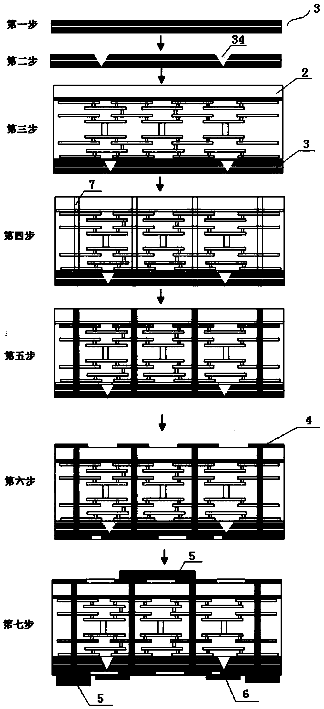
[0024] The present invention will be further described in detail below in conjunction with the accompanying drawings and specific embodiments.

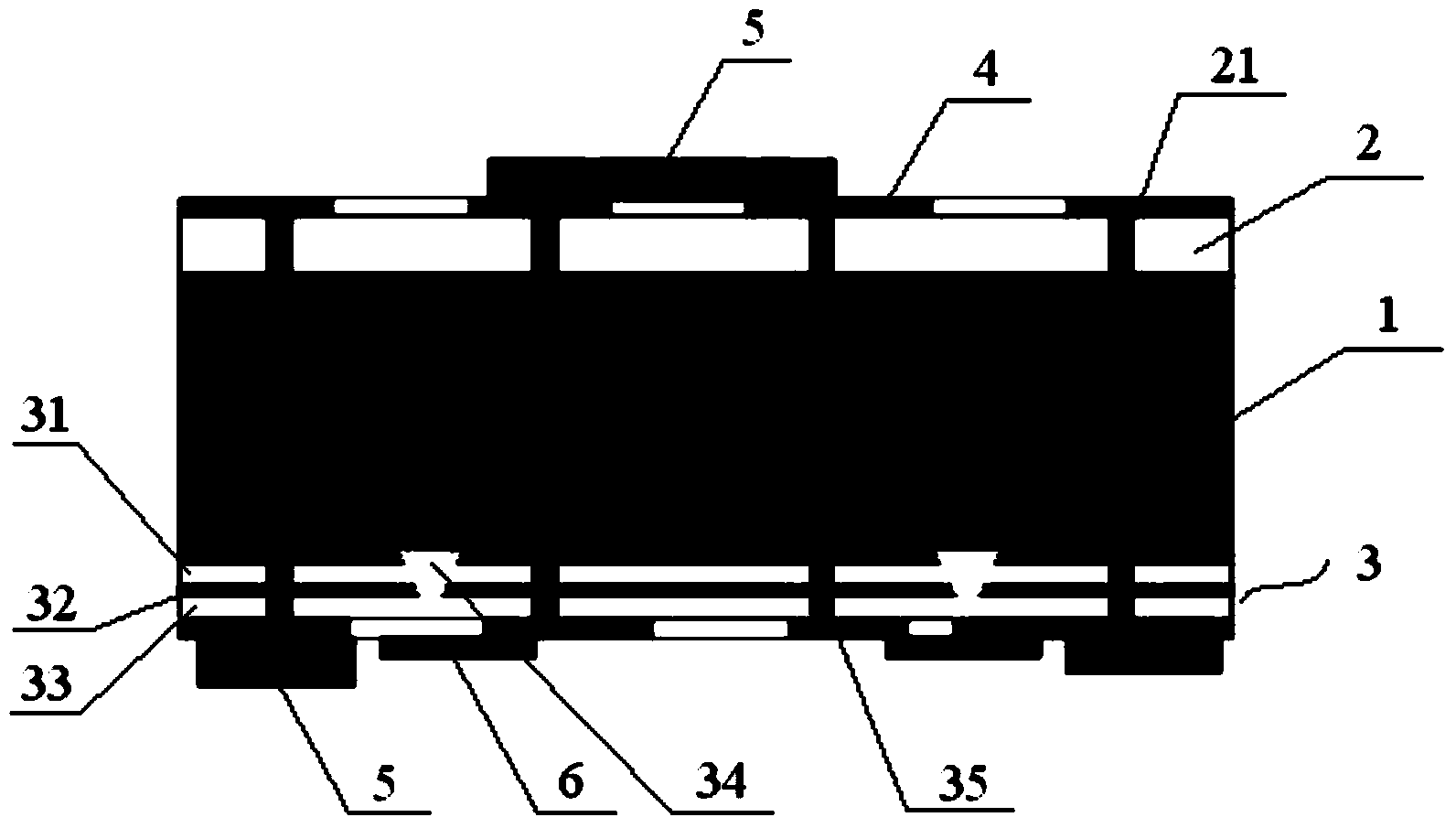
[0025] A multifunctional substrate compatible with PCB technology, its structure is as follows figure 1 As shown, it includes a multilayer interconnection substrate 1 , a glass substrate 2 and an optical waveguide layer 3 .

[0026] Wherein the glass substrate 2 is pressed on the upper end surface of the multilayer interconnection substrate 1 , and the upper surface of the glass substrate 2 is etched with an upper layer pattern. An electronic device 5 is welded on the upper pattern on the upper surface of the glass substrate, and the electronic device is sealed with a glass cover.

[0027] The optical waveguide layer 3 is pressed on the lower end surface of the multilayer interconnection substrate 1. The optical waveguide layer 3 includes an upper cladding layer 31, an optical waveguide core layer 32, and a lower cladding layer 33; ...


PUM


Abstract

The invention discloses a multifunctional base plate based on the PCB technology and a manufacturing method thereof. The multifunctional base plate comprises a multilevel interconnection base plate, a glass base plate and an optical waveguide layer. An upper-layer graph is etched on the upper surface of the glass base plate, and a del-shaped reflector is arranged in the optical waveguide layer. A lower-layer graph is etched on the lower surface of the optical waveguide layer, and the upper-layer graph and the lower-layer graph are communicated with a transmission channel of the multilevel interconnection base plate through through holes vertically formed in the glass base plate, the multilevel interconnection base plate, and the optical waveguide layer in an embedded mode. The manufacturing method includes the steps of pressing the glass base plate and the optical waveguide layer, cutting the reflector, manufacturing the through holes, hole plating copper and face copper, etching the graphs and bonding pads and installing devices. The multifunctional base plate based on the PCB technology and the manufacturing method thereof can solve the problem of low losses of high-frequency transmission, so that the optical interconnection transmission capacity is high, the interconnection density is high, and the anti-electromagnetic interference capability is high; the multifunctional base plate based on the PCB technology and the manufacturing method thereof are suitable for millimeter wave interconnection, the manufacturing technology is simple, cost is low, and the multifunctional base plate based on the PCB technology and the manufacturing method thereof are also suitable for application with the sealing requirement.

Description

technical field [0001] The invention relates to the technical field of integrated electronics, in particular to a hybrid integrated packaging device and a manufacturing method thereof. Background technique [0002] Most of the existing integrated circuits are two-dimensional integrated circuits, and two-dimensional integrated circuits refer to the distribution of various components of the integrated circuit on a plane one by one. With the continuous improvement of integration, the number of device units on each chip increases sharply, the chip area increases, and the growth of inter-unit connections not only affects the working speed of the circuit but also takes up a lot of area, which seriously affects the further improvement of integration and working speed of integrated circuits. Thus, a new technical idea of ​​3D integration is generated. The overlapping structure of three-dimensional integrated circuit multilayer devices can double the integration of the chip. The ove...

Claims


Application Information

Patent Timeline
Patent Type & Authority Applications(China)
IPC IPC(8): H01L23/498H01L23/538H01L21/48G02B6/122G02B6/13
CPCH01L2924/0002H01L2924/00
Inventor 刘丰满李宝霞何晓峰曹立强
Owner NAT CENT FOR ADVANCED PACKAGING
Why Eureka
Try Eureka