Aluminum-substrate-based three-dimensional lamination chip packaging structure and preparation method thereof

A packaging structure, aluminum substrate technology, applied in semiconductor/solid-state device manufacturing, electrical components, electrical solid-state devices, etc., can solve the problems of poor heat dissipation, large CTE mismatch, large line spacing, etc., to improve interconnection density, improve Packaging efficiency, the effect of increasing heat dissipation

Active Publication Date: 2015-11-04
SHANGHAI SPACEFLIGHT ELECTRONICS & COMM EQUIP RES INST
View PDF6 Cites 6 Cited by
  • Summary
  • Abstract
  • Description
  • Claims
  • Application Information

AI Technical Summary

Problems solved by technology

The co-fired ceramic substrate is affected by the process, and the line spacing is large, which cannot meet the needs of high-density substrates. The poor heat dissipation and large shrinkage affect its use in high-power high-frequency device packaging; the organic packaging substrate and chip Large CTE mismatch, more sensitive to moisture, affecting the reliability of the packaging structure
Glass substrates face the problems of high processing difficulty and high cost
The three-dimensional stacked chip package based on the assembly of packaged chips often uses Kovar alloy as the carrier of the chip. Kovar has a relatively large proportion and has little effect on further reducing the volume and weight of the package.

Method used


Image

  • Aluminum-substrate-based three-dimensional lamination chip packaging structure and preparation method thereof
  • Aluminum-substrate-based three-dimensional lamination chip packaging structure and preparation method thereof
  • Aluminum-substrate-based three-dimensional lamination chip packaging structure and preparation method thereof

Examples


Embodiment 1

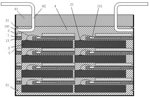
[0059] combine figure 1 , this embodiment describes in detail the schematic diagram of the packaging structure of the three-dimensional laminated chip based on the aluminum substrate of the present invention, which includes: at least two layers of functionalized aluminum substrates 1 arranged in parallel, chips 2, aluminum-based dams 3, epoxy resin The substrate 4, the side metallized interconnection layer 5 and the signal lead-out layer. In this embodiment, the functionalized aluminum substrate 1 arranged in parallel with three layers is taken as an example. The functionalized aluminum substrate 1 has two opposite surfaces, which are respectively the first surface 11 and the second surface. Two surfaces 12, the functionalized aluminum substrate 1 is provided with a buried aluminum interconnection layer 13 and a through hole 14; the buried aluminum interconnection layer 13 is embedded in the functionalized aluminum substrate 1; the through hole 14 penetrates the first surface o...

Embodiment 2

[0068] combine Figure 4 -5. This embodiment describes in detail the preparation method of the packaging structure of the three-dimensional laminated chip based on the aluminum substrate of the present invention, such as Figure 4 Shown is its flowchart, which includes the following steps:

[0069] S11: Preparation of functionalized aluminum substrate: provide a double polished aluminum substrate, the aluminum substrate has two opposite first surfaces and second surfaces, carry out wiring design on the first surface and the second surface by photolithography process, and pass A buried aluminum interconnection layer embedded in the aluminum substrate is prepared on the aluminum substrate by anodic oxidation. One end of the buried aluminum interconnection layer exposes the first surface of the aluminum substrate, and the preparation of the functionalized aluminum substrate is completed. The corresponding functionalized aluminum substrate Schematic such as Figure 5a shown;

...


PUM


Abstract

The invention discloses an aluminum-substrate-based three-dimensional lamination chip packaging structure and a preparation method thereof. The structure comprises at least two layers of functionalized aluminum substrates, chips, aluminum-based dams, epoxy resin base bodies, a side metalized interconnection layer, and a signal leading-out layer. The functionalized aluminum substrates arranged in parallel have two opposite first surfaces and second surfaces. Chips are pasted on the second surfaces. The aluminum-based dams are pasted on the first surfaces. The epoxy resin base bodies are arranged between the functionalized aluminum substrates and the aluminum-based dams. The side metalized interconnection layer and the signal leading-out layer are arranged at the outer sides of the packaging structure in an encircling mode. The functionalized aluminum substrates contain aluminum-buried interconnection layers and through holes; and the chips and the aluminum-buried interconnection layers are electrically connected. Besides, the method includes the steps of preparation of functionalized aluminum substrates, preparation of through holes of the functionalized aluminum substrates, packaging of a multi-chip module, preparation of a signal leading-out layer; packaging of a three-dimensional lamination layer, and preparation of a side metalized interconnection layer. According to the invention, the packaging efficiency and interaction density are improved; and the size of the three-dimensional lamination chip packaging is effectively reduced.

Description

technical field [0001] The invention relates to the field of microelectronic packaging, in particular to a packaging structure of a three-dimensional laminated chip based on an aluminum substrate and a preparation method thereof. Background technique [0002] As microelectronic packaging technology continues to evolve, it presents the challenge of meeting three system metrics: size, performance, and cost. Due to the elimination of individual packages and their parasitic effects, the multichip module (Multichip Module, MCM) has the characteristics of being able to obtain smaller, lighter systems and faster speeds, and has become one of the most cost-effective packaging technologies. [0003] Three-dimensional laminated chip packaging is an effective way to solve the electrical interconnection between chips and chips, and between chips and substrates. It is the development trend of multi-chip modules in the Z direction and is a key technology in the field of microelectronics t...

Claims


Application Information

Patent Timeline
Patent Type & Authority Applications(China)
IPC IPC(8): H01L23/488H01L23/367H01L21/48H01L21/60
CPCH01L2224/48091H01L2924/00014
Inventor 吴伟伟刘米丰曹向荣陈靖张诚王立春
Owner SHANGHAI SPACEFLIGHT ELECTRONICS & COMM EQUIP RES INST
Why Eureka
Try Eureka