Multilayer interconnection structure and method for forming the same

a multi-layer interconnection and structure technology, applied in semiconductor devices, semiconductor/solid-state device details, electrical devices, etc., can solve the problems of signal delay, inability to increase the interconnection density, and the above-described multi-layer interconnection is formed in a lattice pattern, so as to facilitate the formation of the multi-layer interconnection structure. , the effect of easy formation

Inactive Publication Date: 2005-12-29
FUJITSU SEMICON LTD
View PDF11 Cites 6 Cited by
  • Summary
  • Abstract
  • Description
  • Claims
  • Application Information

AI Technical Summary

Benefits of technology

[0018] The present invention further provides a FIB (fine ion beam) apparatus for easily forming the multilayer interconnection structure, the apparatus comprising a control unit and a processing unit. The processing unit includes a beam irradiation mechanism, and a control mechanism for controlling the angle of a semiconductor substrate. The semiconductor substrate is inclined to make the body diagonal ver

Problems solved by technology

However, the above-described multilayer interconnection has the limitation that it is formed in a lattice pattern.
As a result, the interconnection resistance and interconnection capacity are increased to cause a signal delay.
Since the additional lower interconnection is required, arrangement of the lower interconnection layer has no degree o

Method used


Image

  • Multilayer interconnection structure and method for forming the same
  • Multilayer interconnection structure and method for forming the same
  • Multilayer interconnection structure and method for forming the same

Examples


first embodiment

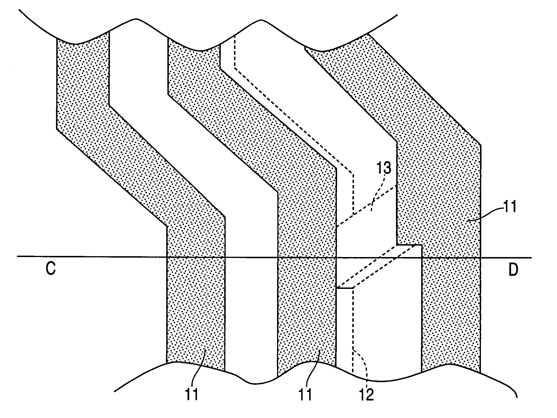
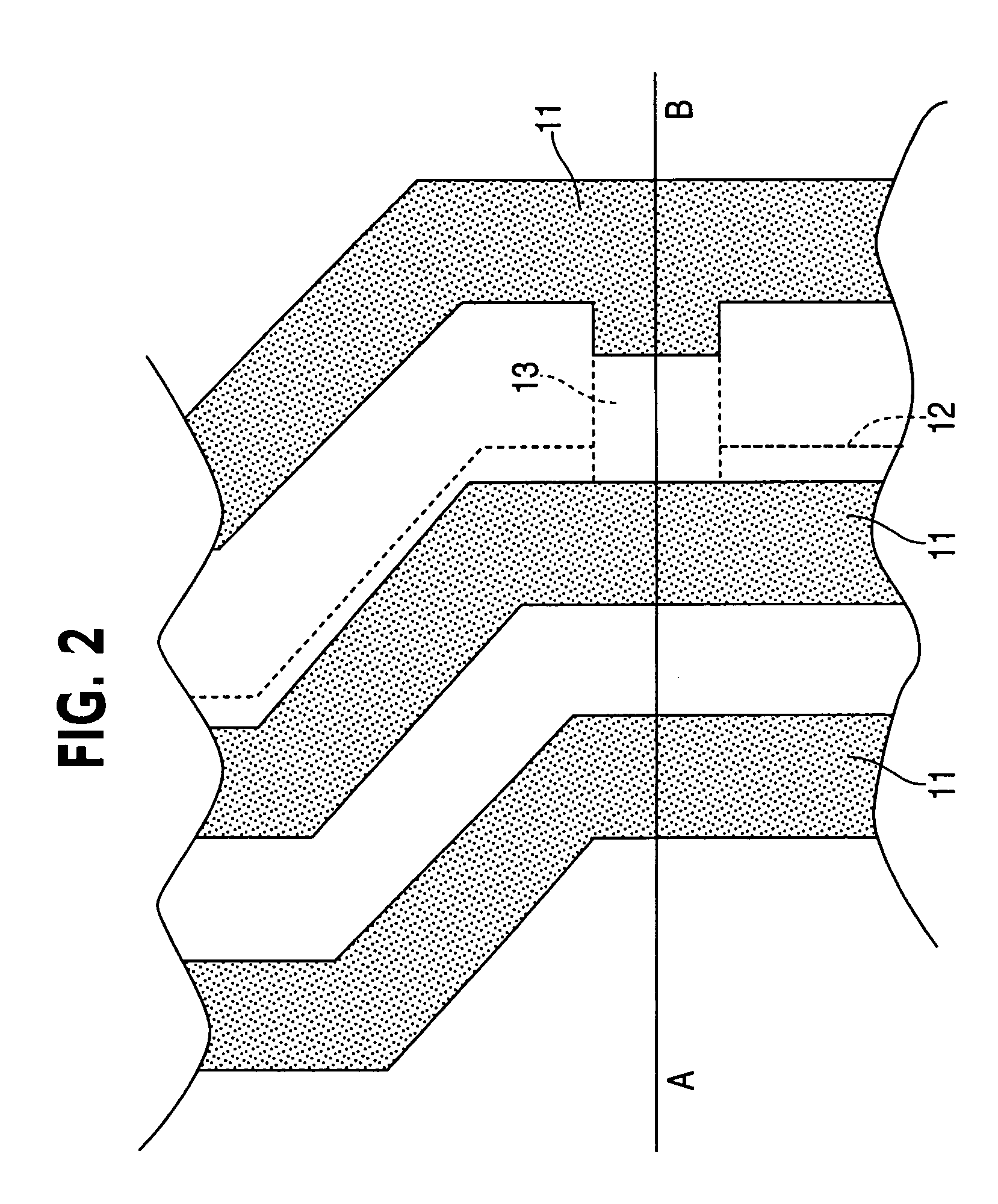
(Multilayer Interconnection Structure Comprising Lower and Upper Interconnection Layers Connected by Connecting Interconnection Including Interconnection Along a Body Diagonal)

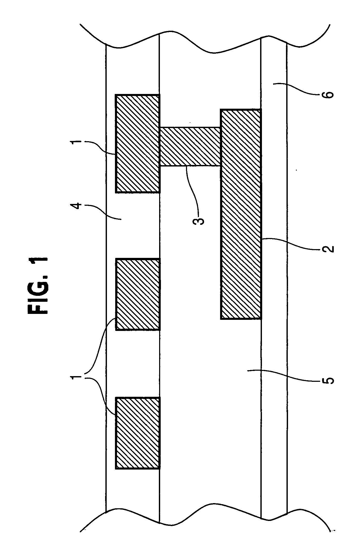
[0040] As shown in FIG. 1, a conventional multilayer interconnection structure comprises a lower interconnection layer 2, an upper interconnection layer 1, connecting interconnection 3, interlayer insulation layers 4 and 5, and an insulation layer 6. In the conventional multilayer interconnection structure, the upper and lower interconnection layers 1 and 2 are connected by the following structure. First, it is necessary to provide the connecting interconnection 3 which vertically extends from the upper interconnection layer 1. Next, in order to connect the lower interconnection layer 2 to the connecting interconnection 3 vertically extending from the upper interconnection layer 1, the lower interconnection layer 2 is required to have a line extending to the point of connection with the connecting interconne...

second embodiment

(Method 1 for Forming the Multilayer Interconnection Structure of the First Embodiment: Forming the Connecting Interconnection Including Interconnection Along the Body Diagonal After Forming Lower and Upper Interconnection Layers)

[0062] In the second embodiment, a first method for forming the multilayer interconnection (or wiring) structure of the first embodiment is described with reference to FIGS. 6A to 6F.

[0063] As shown in FIG. 6A, a step of forming a lower interconnection layer 20 is performed by a so-called damascene process as described below. First, a silicon oxide (SiO2) insulation layer 21 is deposited on a semiconductor substrate. Next, photoresist is coated on the insulation layer 21 and patterned for forming a groove for the lower interconnection layer 20. Next, the silicon oxide (SiO2) insulation layer 21 is etched by reactive ion etching to form the groove for the lower interconnection layer 20, and then the photoresist is removed. Next, a tantalum (Ta) layer is d...

third embodiment

(Method 2 for Forming the Multilayer Interconnection Structure of the First Embodiment: Forming the Connecting Interconnection Including Interconnection Along the Body Diagonal After Forming the Lower and Upper Interconnection Layers)

[0071] In a third embodiment, a second method for forming the multilayer interconnection (or wiring) structure of the first embodiment is described with reference to FIGS. 7A to 7H.

[0072] First, in order to form a lower interconnection layer 35 by a so-called damascene process as shown in FIG. 7A, an insulation layer 36 is deposited on a semiconductor substrate. Then, the lower interconnection layer 35 is formed by the same step as shown in FIG. 6A.

[0073] Next, as shown in FIG. 7B, in order to form an interlayer insulation layer, a first silicon nitride (SiN) layer 38 and a first silicon oxide (SiO2) layer 37 are deposited in that order.

[0074] Next, as shown in FIG. 7C, in order to form inclined surfaces in the first silicon oxide (SiO2) layer 37, ...


PUM


Abstract

A multilayer interconnection structure of the present invention includes first interconnection, second interconnection belonging to an interconnection layer different from an interconnection layer to which the first layer belongs, and third interconnection for connecting the first and second interconnections, the third interconnection belonging to a different interconnection layer and including interconnection along a body diagonal for connecting two points in different planes belong to different interconnection layers. A method for producing the multilayer interconnection structure includes a step of forming the third interconnection, the step including a step of forming a through hole along the body diagonal, and a step of filling the through hole with a conductive material.

Description

CROSS-REFERENCE TO RELATED APPLICATIONS [0001] This application is based upon and claims the benefit of priority from the prior Japanese Patent Application No. 2004-187005, filed on 2004 Jun. 24, the entire contents of which are incorporated herein by reference. BACKGROUND OF THE INVENTION [0002] 1. Field of the Invention [0003] The present invention relates to a multilayer interconnection structure of a semiconductor device in which different interconnection layers of multilayer interconnection are connected at predetermined positions, and a method for forming the multilayer interconnection structure. In particular, the present invention relates to a multilayer interconnection structure of a semiconductor device, the multilayer interconnection structure including a connecting interconnection for connecting predetermined two points of different interconnection layers of multilayer interconnection structure with a short distance therebetween. [0004] 2. Description of the Related Art ...

Claims


Application Information

Patent Timeline
IPC IPC(8): H01L21/285H01L21/44H01L21/768H01L23/48H01L23/52H01L23/522H01L29/40
CPCH01L21/28562H01L21/76804H01L21/76879H01L21/76895H01L2924/0002H01L23/5226H01L2924/00H01L21/76816
Inventor KATASE, SYUJISUZUKI, KOUICHICHICHII, KENJITABARA, KATSUJI
Owner FUJITSU SEMICON LTD
Why Eureka
Try Eureka