Method of assembly for multi-flip chip on lead frame on overmolded IC package

a technology of lead frame and ic package, which is applied in the direction of semiconductor devices, semiconductor/solid-state device details, electrical apparatus, etc., can solve the problems of not being able to use, requiring special lead frame, and other packages not providing a molded encapsulant for the integrated circuit. , to achieve the effect of improving performance, improving signal integrity, and high interconnect density

Inactive Publication Date: 2008-02-26
SEMICON COMPONENTS IND LLC
View PDF20 Cites 7 Cited by
  • Summary
  • Abstract
  • Description
  • Claims
  • Application Information

AI Technical Summary

Benefits of technology

[0009]In order to overcome the drawbacks of the prior art and provide systems with improved signal integrity, we have invented a multichip package and packaging method that relies upon proven technology familiar to manufacturers. Our invention uses a standard package foot print that enables customers to readily incorporate multichip modules into their existing systems. Our invention achieves improved performance by closely locating the system die to each other to provide short interconnection length. The invention provides a high interconnect density and reduces the space needed on a printed circuit board for the circuits that populate the board. The invention also provides lower power consumption by requiring smaller drivers. It may be used for mixed signal applications, saves package costs and is faster to bring a given multichip module to market.

Problems solved by technology

Some are complex and require special leadframes with conductive vias.
Others package only two chips so that they cannot be used for applications that require multiple mosfets and a controller.
Other packages do not provide a molded encapsulant for the integrated circuit.
Signal integrity is a major design problem in complex systems that run at high speed and include logic and power devices.
If the lead or trace has too high a resistance, the system may fail or malfunction.

Method used


Image

  • Method of assembly for multi-flip chip on lead frame on overmolded IC package
  • Method of assembly for multi-flip chip on lead frame on overmolded IC package
  • Method of assembly for multi-flip chip on lead frame on overmolded IC package

Examples


Embodiment Construction

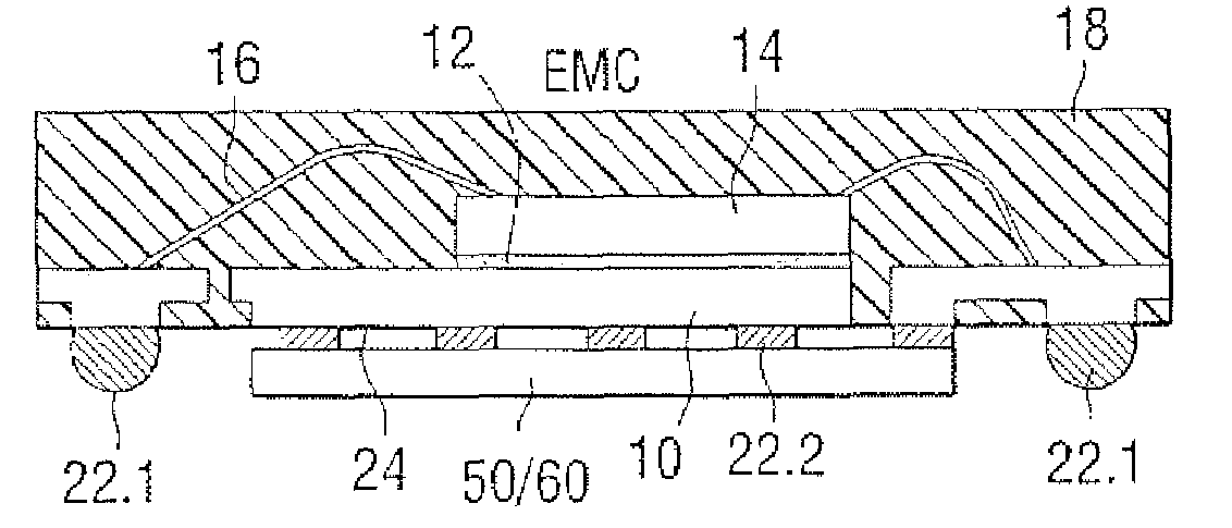
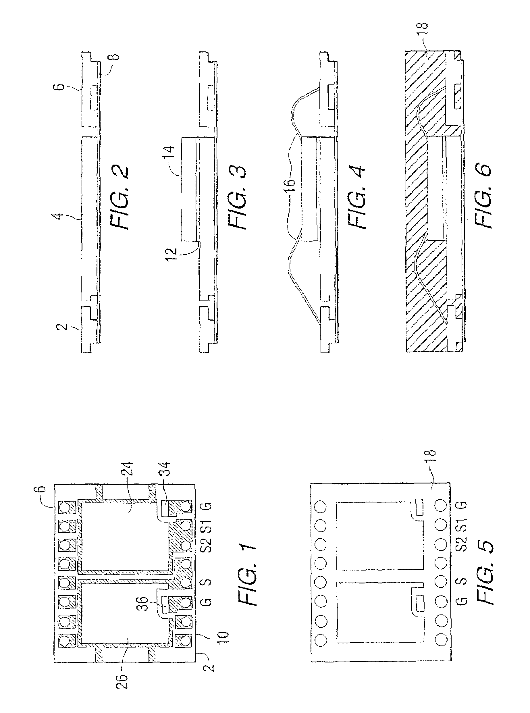
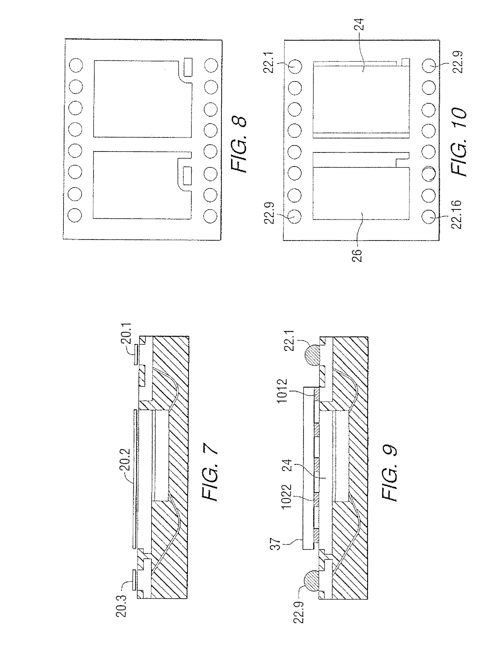
[0039]A known method of forming a flip chip on leadframe semiconductor package employs a plated leadframe. A leadframe is a patterned sheet of metal, typically copper, that has been plated, usually with silver, nickel or palladium. Conventionally, a leadframe is plated to prevent the copper from oxidizing, and to provide a surface to which solder will adhere. The pattern of the sheet of metal provides a leadframe for forming a semiconductor package.

[0040]The leadframe 10 of FIG. 1 holds a controller integrated circuit on one side and high and low side mosfets on the other side to provide a multichip module with logic and power devices. The leadframe 10 has source pads 24, 26 for receiving source studs and inner leads 34, 36 for receiving the gate studs. The inner source pads 24, 26 are integral with outer source leads 124, 126 respectively, for connecting the sources of the mosfets to the outer leads. The inner gate leads 34, 36 are integral with outer gate leads 134, 136, respectiv...


PUM


Abstract

A multichip module package uses bond wire with plastic resin on one side of a lead frame to package an integrated circuit and flip chip techniques to attach one or more mosfets to the other side of the lead frame. The assembled multichip module 30 has an integrated circuit controller 14 on a central die pad. Wire bonds 16 extend from contact areas on the integrated circuit to outer leads 2.6 of the lead frame 10. On the opposite, lower side of the central die pad, the sources and gates of the mosfets 24, 26 are bump or stud attached to the half etched regions of the lead frame. The drains 36 of the mosfets and the ball contacts 22.1 on the outer leads are soldered to a printed circuit board.

Description

CROSS-REFERENCE TO RELATED APPLICATIONS[0001]This application is a Divisional of and claims priority from U.S. patent application Ser. No. 10 / 803,464, filed Mar. 18, 2004 now U.S. Pat. No. 7,154,186.FIELD OF THE INVENTION[0002]This invention relates to semiconductor packaging and, in particular, to a multichip package with two or more mosfets and a mosfet controller integrated circuit.BACKGROUND[0003]Power mosfets are ubiquitous in modern electronic systems. They provide the power to motors and actuators in automobiles and to electronic displays including computer terminals and cell phones. There is a constant demand to make electronic systems perform more functions, take us less space and be more reliable. Customers of integrated circuit and mosfet manufacturers want an integrated solution in a single chip or single module that includes not only the power mosfets needed for the system, but also the controller integrated circuit for operating the mosfets. An ideal solution would be ...

Claims


Application Information

Patent Timeline
Patent Type & Authority Patents(United States)
IPC IPC(8): H01L21/44H01L21/48H01L23/31H01L23/495H01L23/52H01L25/16
CPCH01L23/3128H01L23/49575H01L24/97H01L25/16H01L2224/16H01L2224/32245H01L2224/48091H01L2224/48247H01L2224/48472H01L2224/73265H01L2224/92247H01L2224/97H01L2924/01013H01L2924/01029H01L2924/01046H01L2924/01047H01L2924/01078H01L2924/01079H01L2924/01082H01L2924/13091H01L2924/15311H01L2924/1532H01L2924/00014H01L2224/85H01L2224/83H01L24/48H01L2924/01006H01L2924/01033H01L2924/00H01L2224/45144H01L2924/00012H01L2224/45124H01L2924/181H01L2924/12042H01L24/45H01L24/73H01L2924/14H01L2224/05599
Inventor NOQUIL, JONATHAN A.CHOI, SEUNG YONGJOSHI, RAJEEVWU, CHUNG-LIN
Owner SEMICON COMPONENTS IND LLC
Why Eureka
Try Eureka