High reliability multilayer circuit substrates and methods for their formation

a multi-layer circuit and substrate technology, applied in the field of semiconductor device fabrication, can solve the problems of limiting the usefulness of multi-layer substrates formed by high temperature processing, limiting the use of refractory substrates, and complex hybrid circuits that typically require equally complex interconnection structures, etc., to achieve the effect of facilitating the production of highly reliable substrates, reducing or eliminating the yield of misalignment, and high tunable properties

Inactive Publication Date: 2005-07-07
MEDTRONIC MIMIMED INC
View PDF5 Cites 5 Cited by
  • Summary
  • Abstract
  • Description
  • Claims
  • Application Information

AI Technical Summary

Benefits of technology

[0014] In accordance with embodiments of the invention, a multilayer circuit substrate is comprised of a base substrate and one or more additional dielectric and conductive thin films formed over the base substrate by vacuum deposition methods. The vacuum deposited dielectric layers are significantly thinner than the dielectric layers used in conventional lamination techniques, allowing for the formation of multilayer circuit substrates that are significantly thinner than those formed by conventional lamination techniques. Because vacuum deposited dielectrics are deposited in an “as-fired” state that undergoes essentially no shrinkage during subsequent processing, yield reduction due to misalignment is significantly reduced or eliminated. In addition, vacuum deposition techniques do not impose limitations on the types of conductors or dielectric materials that may be employed, enabling the use of a wide variety of materials with highly tunable properties. Vacuum deposition techniques also produce hermetic layers that facilitate the production of highly reliable substrates.
[0015] In accordance with further embodiments of the invention, deposited dielectrics may be patterned through the use of sacrificial structures that may be removed using highly selective etch chemistry. The sacrificial structures are preferably formed using a high precision shadow mask that allow dielectric patterns to be precisely registered to underlying structures and thus enabling high interconnect densities and narrow dimensional tolerances not achievable by conventional lamination techniques.
[0017] In accordance with further embodiments of the invention, hermetic vias may be formed in the dielectric base substrate by forming successive thin layers of a conductive material on the sidewalls of a via hole using a dilute conductive ink, followed by formation of a conductive plug using a concentrated conductive ink. The conductive material in the via is then sintered to form a unitary body, producing a hermetic via without shrinkage of the surrounding dielectric.

Problems solved by technology

Complex hybrid circuits typically require equally complex interconnection structure.
Various conventional lamination techniques are known, however each has limitations that restricts its usefulness for producing multilayer substrates.
As a result, substrates formed by high temperature processing are limited to the use of refractory metal conductors such as tungsten and molybdenum, which have very low resistance to corrosion in the presence of moisture and are therefore not appropriate for use in harsh environments.
However the dielectric materials used in low-temperature processes are generally provided with a high glass content and therefore have relatively poor resistance to environmental corrosion, as well as a relatively low dielectric constant and relatively poor thermal conductivity.
However, thick film techniques require the use of relatively thick dielectric layers and thus it is difficult to produce a thin multilayer substrate using thick film techniques.
Thick film dielectrics also have relatively low dielectric constants, relatively poor thermal conductivity, and poor corrosion resistance.
In addition to the problems listed above, the conventional lamination techniques cannot use green sheets of less than 0.006 inches in thickness because thinner green sheets cannot reliably survive necessary processing such as drilling or punching of via holes.
Also, because the designer has limited control over the thickness of individual green sheets, the number of layers of the multilayer substrate is often limited according to the maximum allowable substrate thickness for the intended application.
Thus, where a thin multilayer substrate is desired, lamination techniques generally do not provide optimal results.
In addition, the firing required in the conventional lamination techniques can cause shrinkage in excess of 10% in both dielectric and conductor materials, which can produce distortions that result in misalignment of vias and conductors after firing.
While shrinkage effects can be addressed to some extent during design for substrates having a modest interconnect density, the design process is made more time consuming and a significant reduction in yield may occur in applications with higher densities and tighter dimensional tolerances.
The conventional technology is therefore limited by several restrictions.
All of the aforementioned techniques are limited with respect to the minimum substrate thicknesses that can be produced, and the various firing requirements of the aforementioned techniques prevent the use of materials that are desirable for circuit structures.
All of the aforementioned techniques also suffer from shrinkage during firing that causes alignment problems.

Method used


Image

  • High reliability multilayer circuit substrates and methods for their formation
  • High reliability multilayer circuit substrates and methods for their formation
  • High reliability multilayer circuit substrates and methods for their formation

Examples


Embodiment Construction

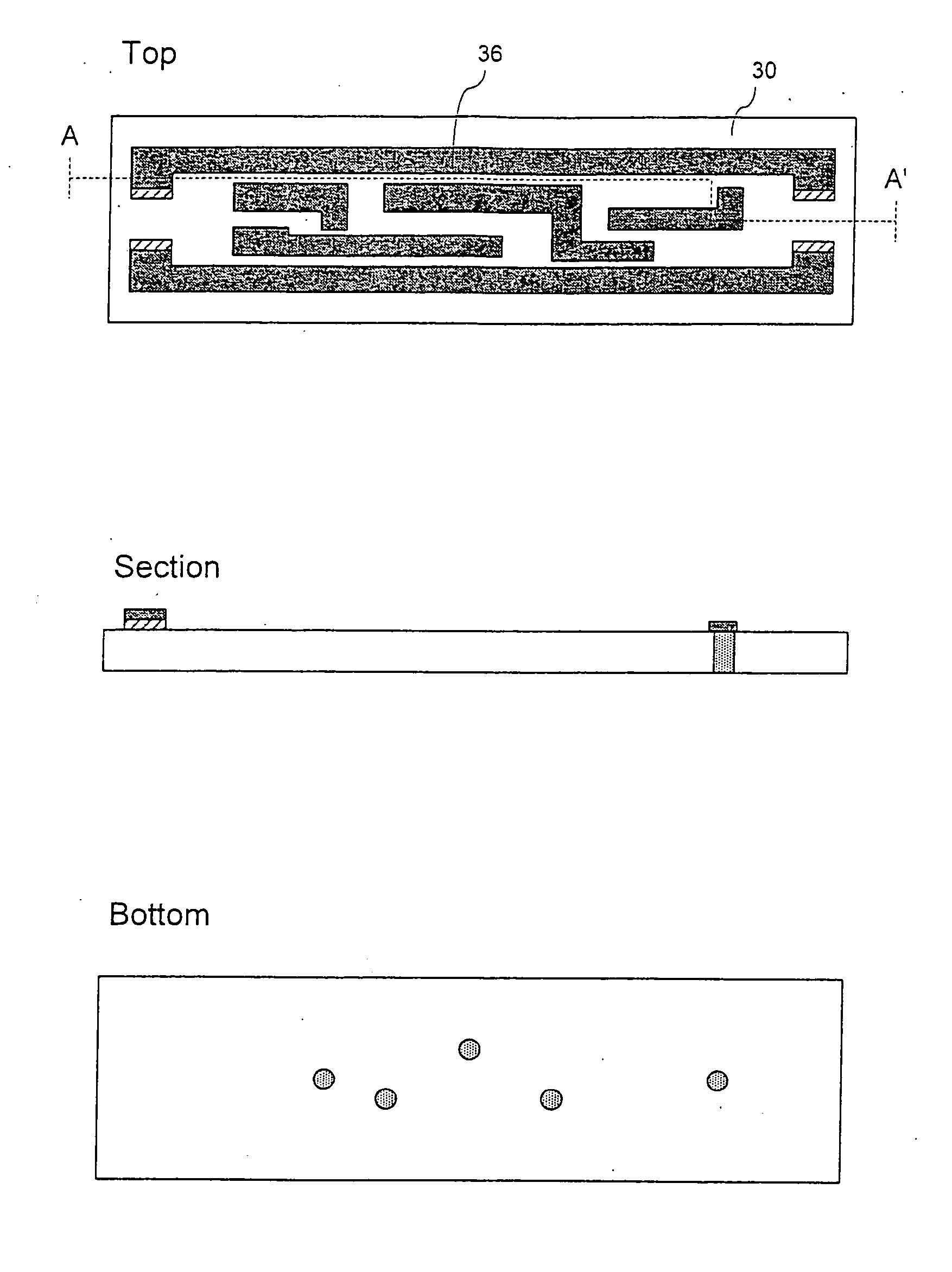
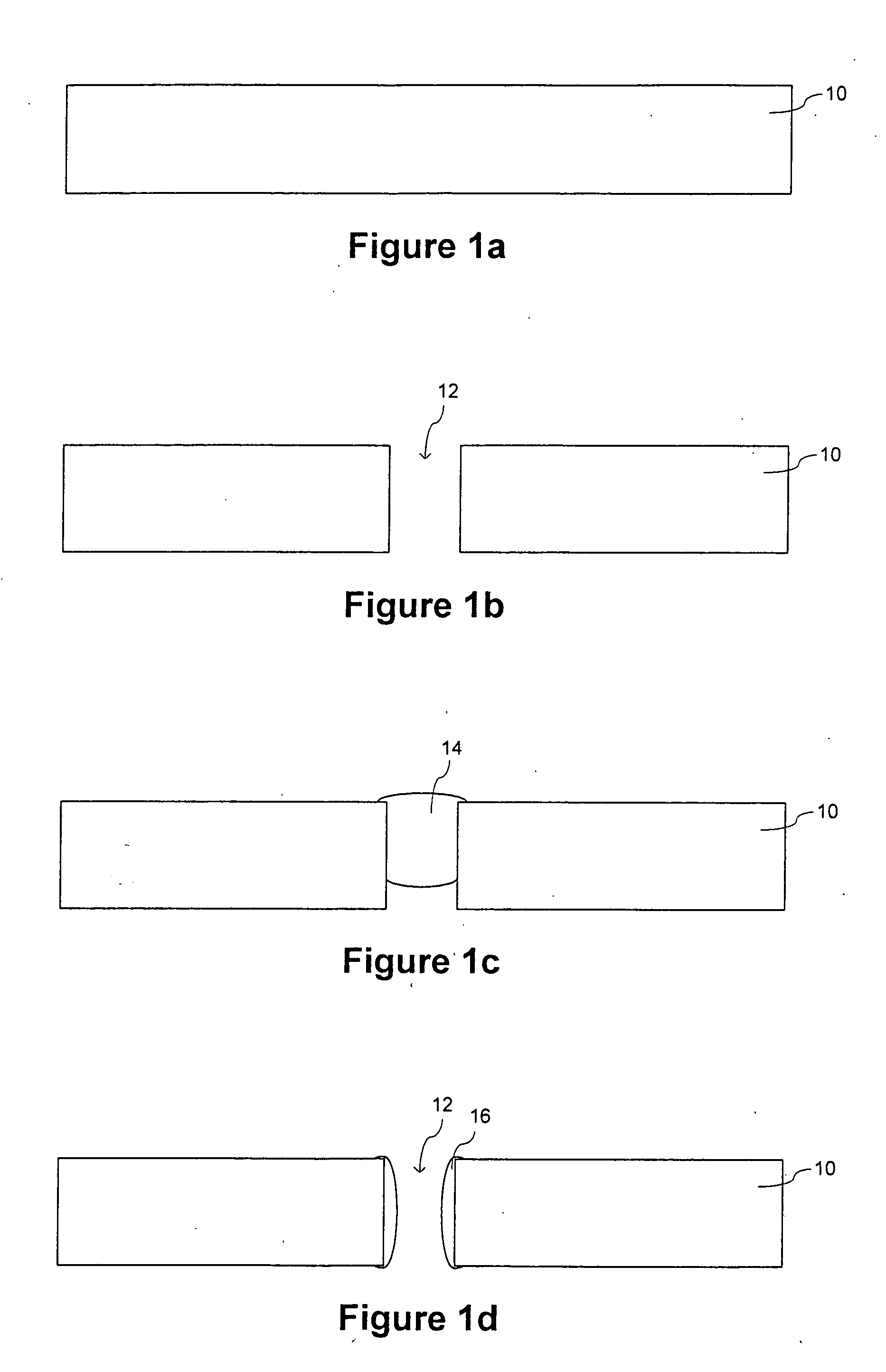
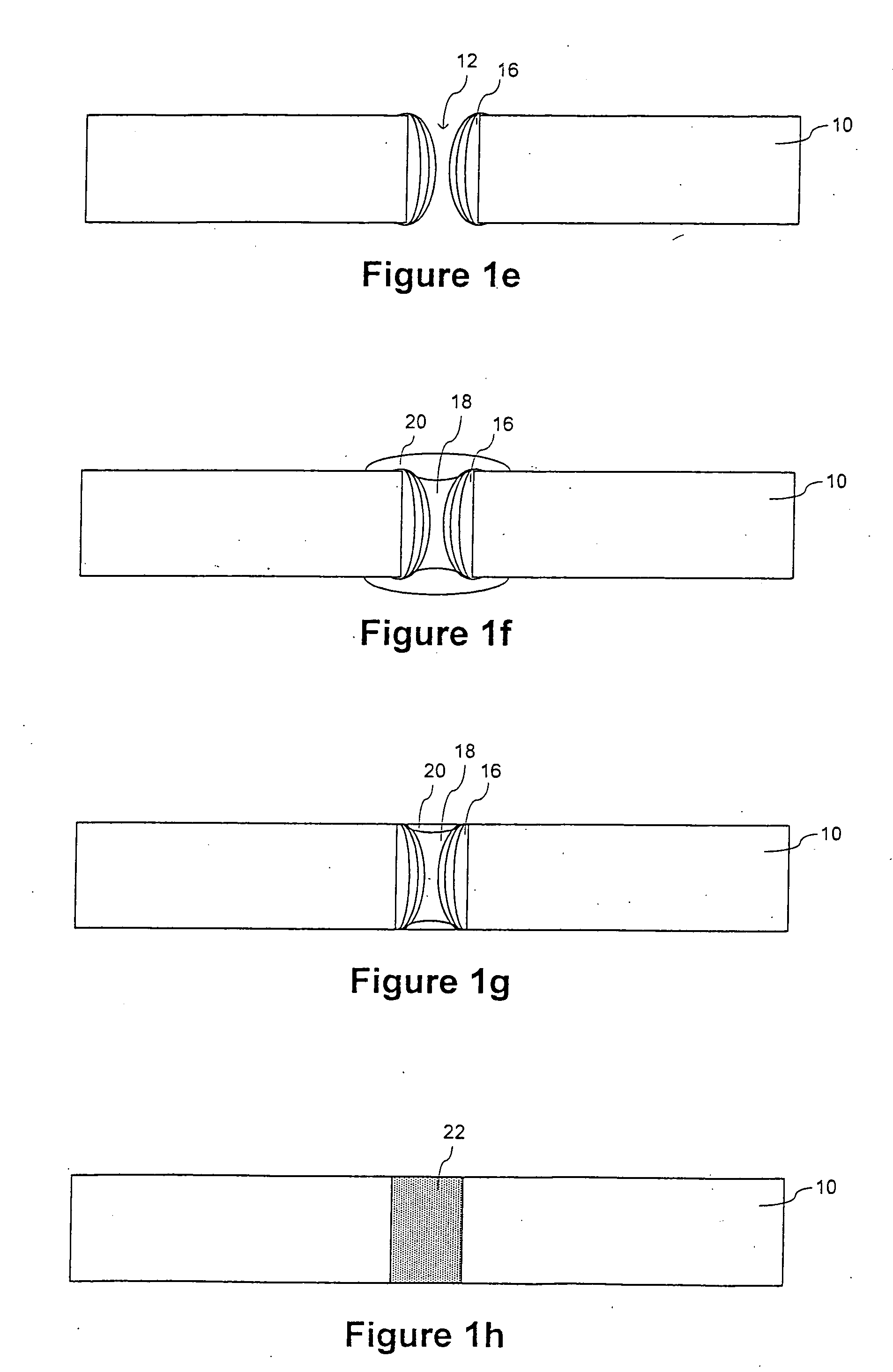
[0023] A preferred embodiment of a method for producing a multilayer circuit substrate is now described in the context of production of a hermetic blood glucose sensor circuit. It should be understood that the processing performed in the preferred embodiment represents one implementation of the invention and that the techniques of the invention have a variety of alternative applications, examples of which are provided after the description of the preferred embodiment.

[0024]FIGS. 1a-1h show structures formed during processing in accordance with the preferred embodiment to form a hermetic via in a dielectric base substrate. While the processing of FIGS. 1a-1h illustrates a single via, it will be appreciated that multiple vias may be produced simultaneously using the illustrated techniques.

[0025]FIG. 1a shows a cross-sectional view of a portion of a dielectric base substrate 10. The base substrate is preferably a sheet of 96% purity alumina (Al2O3) that is pre-fired such that shrinka...


PUM

PropertyMeasurementUnit
thicknessaaaaaaaaaa
shrinkageaaaaaaaaaa
shrinkageaaaaaaaaaa

Abstract

A multilayer circuit substrate for multi-chip modules or hybrid circuits includes a dielectric base substrate, conductors formed on the base substrate and a vacuum deposited dielectric thin film formed over the conductors and the base substrate. The vacuum deposited dielectric thin film is patterned using sacrificial structures formed by shadow mask techniques. Substrates formed in this manner enable significant increases in interconnect density and significant reduction of over-all substrate thickness.

Description

RELATED APPLICATIONS [0001] This application claims priority under 35 USC §119(e) from U.S. Provisional Application Ser. No. 60 / 414,289, filed 27 Sep. 2002, entitled “Multilayer Substrate,” the entirety of which is incorporated herein by reference. [0002] This application is a continuation-in-part claiming priority under 35 USC §120 from U.S. patent application Ser. No. 10 / 331,186, filed 26 Dec. 2002, entitled “Multilayer Substrate,” the entirety of which is incorporated herein by reference. [0003] This application related to U.S. patent application Ser. No. 10 / 038,276, filed 31 Dec. 2001, entitled “Sensor Substrate and Method of Fabricating Same,” the entirety of which is incorporated herein by reference.BACKGROUND [0004] 1. Field of the Invention [0005] Embodiments of the invention relate to semiconductor device fabrication, and, in particular, to the formation of multilayer wiring substrates on which integrated circuits or discrete devices are mounted. [0006] 2. Description of Re...

Claims


Application Information

Patent Timeline
Patent Type & Authority Applications(United States)
IPC IPC(8): H01L21/48H05K1/16H05K3/04H05K3/40H05K3/46
CPCH01L21/4857H01L2924/19107H05K1/162H05K3/048H05K3/4053H05K3/4061H05K3/4664H05K3/467H05K2201/0179H05K2203/0278H05K2203/085H05K2203/1476H05K2203/308H01L2924/0002H01L21/4867H01L2924/00
Inventor SHAH, RAJIVPENDO, SHAUN
Owner MEDTRONIC MIMIMED INC
Why Eureka
Try Eureka