Anti-drifting structure for soldering tin of electronic component

An electronic component, anti-drift technology, applied in the direction of electrical components, electrical connection printed components, printed circuits connected to non-printed electrical components, etc., can solve the problem of insufficient regional strength, component position deviation, and product yield decline and other problems, to achieve the effect of increasing the pin contact area, improving the yield rate, and increasing the echo resistance.

Inactive Publication Date: 2022-02-11
ZHUHAI HUACUI TECH CO LTD
View PDF10 Cites 0 Cited by
  • Summary
  • Abstract
  • Description
  • Claims
  • Application Information

AI Technical Summary

Problems solved by technology

[0003] However, if the components are refined or the substrate is flexible, it is easy to encounter problems due to the need to improve the alignment accuracy and the expansion and contraction of the flexible substrate; during reflow soldering, the position of the components will shift and drop, resulting in product yield decline
[0004] Generally, solder paste is applied on the patterned circuit of the copper foil substrate by screen printing or stencil printing, commonly known as the pad, because the solder paste on the pad has undergone a high-temperature reflow process, the pad will also be affected by the solder paste The relationship between high-temperature melting and polymer solvent volatilization leads to component movement and offset. In many designs, the edge of the pad and the current-carrying line is designed at a vertical right angle, resulting in insufficient strength in this area, and it is easy to cause stress concentration in this area. Fracture issues, especially when flexible substrates are bent

Method used


Image

  • Anti-drifting structure for soldering tin of electronic component
  • Anti-drifting structure for soldering tin of electronic component
  • Anti-drifting structure for soldering tin of electronic component

Examples


Embodiment Construction

[0021] The following will clearly and completely describe the technical solutions in the embodiments of the present invention with reference to the accompanying drawings in the embodiments of the present invention. Obviously, the described embodiments are only some, not all, embodiments of the present invention. Based on the embodiments of the present invention, all other embodiments obtained by persons of ordinary skill in the art without making creative efforts belong to the protection scope of the present invention.

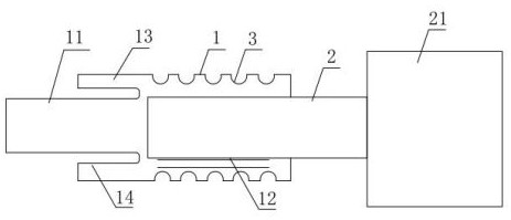
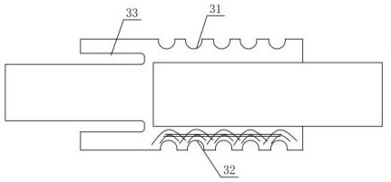
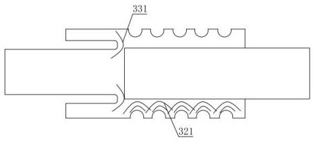
[0022] see Figure 1-Figure 4 , an anti-drift structure for soldering of electronic components, including a pad 1, the tail end of the pad 1 is connected with a power line 11, a welding groove 12 is opened inside the pad 1, and a pin 2 is inserted into the soldering groove 12 An anti-drift component 3 is provided on the pad 1, the anti-drift component 3 includes an upper edge polygon 31, a lower edge polygon 32 and a side edge polygon 33, the upper edge polygo...


PUM


Abstract

The invention discloses an anti-drifting structure for soldering tin of an electronic component, which comprises a bonding pad, the tail end of the bonding pad is connected with a power-on circuit, a welding groove is formed in the bonding pad, a pin is inserted in the welding groove, and an anti-drifting assembly is arranged on the bonding pad; the anti-drifting assembly comprises an upper edge polygon, a lower edge polygon and a side edge polygon, and the upper edge polygon is arranged on the upper side face of the bonding pad. According to the anti-drifting structure for soldering tin of the electronic component, drifting, caused by reflow soldering tin, of the component on a circuit is reduced, the problem of breakage caused by stress concentration is solved, the yield of products is improved, the edge of the weld leg is designed into a polygon, the echo resistance of liquid soldering tin on the edge of the weld leg flowing outwards is increased, reflected waves can be generated; And meanwhile, the contact area of the edge of the welding pin and the pin of the component can be increased, and the opportunity of insufficient welding is avoided.

Description

technical field [0001] The invention relates to the technical field of soldering of electronic components, in particular to an anti-drift structure for soldering of electronic components. Background technique [0002] Generally common LED technology can be used to meet the application of direct-lit backlight film block and front-end display, and the manufacturing process adopts rigid and flexible printed circuit board processes such as PCB and FPC. [0003] However, if the components are refined or the substrate is flexible, it is easy to encounter problems due to the need to improve the alignment accuracy and the expansion and contraction of the flexible substrate; during reflow soldering, the position of the components will shift and drop, resulting in product yield decline. [0004] Generally, solder paste is applied on the patterned circuit of the copper foil substrate by screen printing or stencil printing, commonly known as the pad, because the solder paste on the pad...

Claims


Application Information

Patent Timeline
Patent Type & Authority Applications(China)
IPC IPC(8): H01R4/02H05K1/11H05K1/18
CPCH01R4/029H05K1/182H05K1/116
Inventor 汤立文叶宗和董宇坤尹志安莫春鉴丁武马晓鑫
Owner ZHUHAI HUACUI TECH CO LTD
Why Eureka
Try Eureka