Fan-out type packaging structure and packaging method

A packaging method and packaging structure technology, which are applied in the manufacturing of electrical components, electric solid-state devices, semiconductor/solid-state devices, etc., can solve the problems that the substrate manufacturing process cannot meet the requirements of chips and the high cost, achieve high industrial utilization value, improve the manufacturing process, and reduce the size The effect of package size

Pending Publication Date: 2022-02-25
SJ SEMICON JIANGYIN CORP
View PDF0 Cites 1 Cited by
  • Summary
  • Abstract
  • Description
  • Claims
  • Application Information

AI Technical Summary

Problems solved by technology

[0005] In view of the shortcomings of the prior art described above, the purpose of the present invention is to provide a fan-out packaging structure and packaging method, whi

Method used


Image

  • Fan-out type packaging structure and packaging method
  • Fan-out type packaging structure and packaging method
  • Fan-out type packaging structure and packaging method

Examples


Embodiment 1

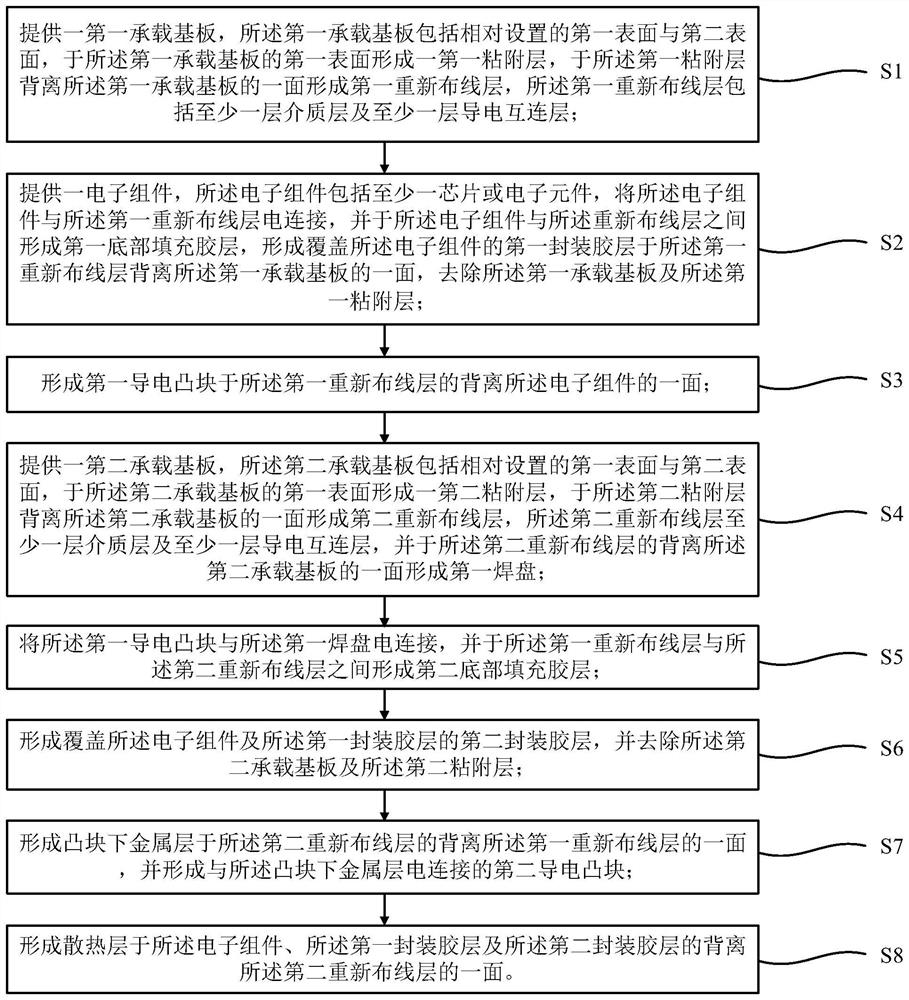
[0089] This embodiment provides a packaging method, such as figure 1 As shown, it is shown as a process flow diagram of the packaging method, including the following steps:

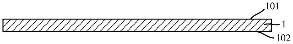
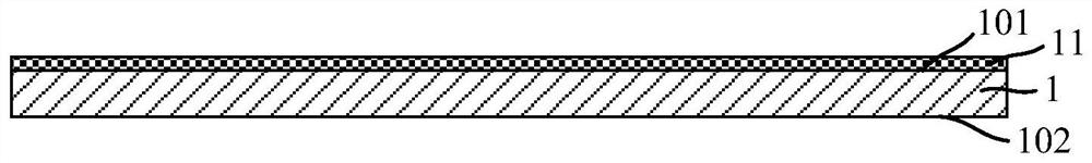
[0090] S1: Provide a first carrier substrate, the first carrier substrate includes a first surface and a second surface oppositely arranged, a first adhesive layer is formed on the first surface of the first carrier substrate, and a first adhesive layer is formed on the first carrier substrate A first rewiring layer is formed on a side of an adhesive layer away from the first carrier substrate, and the first rewiring layer has at least one dielectric layer and at least one conductive interconnection layer;

[0091] S2: Provide an electronic component, the electronic component includes at least one chip or electronic component, electrically connect the electronic component to the first rewiring layer, and form an electronic component and the rewiring layer The first underfill adhesive layer is used to for...

Embodiment 2

[0160] This embodiment provides a fan-out packaging structure, such as Figure 22 As shown, it is a schematic diagram of the cross-sectional structure of the fan-out packaging structure, including the first rewiring layer 12, electronic components 13, the first underfill layer 14, the first packaging adhesive layer 15, the heat dissipation layer 25, the second rewiring layer The wiring layer 22, the second underfill adhesive layer 23 and the second encapsulation adhesive layer 24, wherein the first rewiring layer 12 includes at least one dielectric layer 121 and at least one conductive interconnection layer 122, the first One side of the rewiring layer 12 is provided with a first conductive bump 123; the electronic component 13 is located on the side of the first rewiring layer 12 away from the first underfill glue layer 14, and the electronic component 13 includes at least A chip or an electronic component, the electronic component 13 is electrically connected to the first re...


PUM

PropertyMeasurementUnit
Thicknessaaaaaaaaaa

Abstract

The invention provides a fan-out type packaging structure and packaging method. The packaging structure comprises a first rewiring layer, a first bottom filling adhesive layer, an electronic assembly, a first packaging adhesive layer, a heat dissipation layer, a second rewiring layer, a second bottom filling adhesive layer and a second packaging adhesive layer, wherein the electronic assembly comprises at least one chip or electronic element; and the first packaging adhesive layer wraps the first bottom filling adhesive layer and the side face of the electronic assembly, and the second packaging adhesive layer wraps the first packaging adhesive layer, the second bottom filling adhesive layer and the side face of the first rewiring layer. According to the packaging method, the electronic component is primarily packaged through the first rewiring layer and the first packaging adhesive layer, a traditional substrate is replaced by the second rewiring layer, the primarily packaged electronic component is packaged again through the second rewiring layer and the second packaging adhesive layer, the manufacturing process is improved, and the manufacturing time is shortened; and in addition, high-density integration of devices can be realized, and various electronic components and chips can be packaged at the same time.

Description

technical field [0001] The invention belongs to the field of integrated circuit manufacturing, and relates to a fan-out packaging structure and a packaging method. Background technique [0002] A printed circuit board (PCB for short, also known as a circuit board) is usually used as a support for electronic components and is also a carrier for electrical connections of electronic components. As the basic material of the circuit board, the substrate is mostly applied in batches of 1 to 12 layers. If there are more chip I / Os embedded on the circuit board, the number of substrate layers on the circuit board will increase, and the corresponding The higher the price, and the substrate manufacturing process also has a certain limit. At present, the line width and line spacing of ordinary substrates are usually 50 μm, and the minimum can only reach 20 μm. With the improvement of chip functions and integration, the substrate will not be able to meet the needs of the chip. [0003] ...

Claims


Application Information

Patent Timeline
IPC IPC(8): H01L21/48H01L21/54H01L21/56H01L23/31H01L23/485H01L23/498H01L21/60
CPCH01L21/4857H01L24/83H01L21/54H01L21/56H01L23/49822H01L23/485H01L23/4824H01L23/3121H01L2224/0231H01L2224/02331H01L2224/02333H01L2224/02381H01L2224/02379
Inventor 陈彦亨林正忠
Owner SJ SEMICON JIANGYIN CORP
Why Eureka
Try Eureka