Supercharge Your Innovation With Domain-Expert AI Agents!

Array substrate, preparation method thereof and display panel

A technology of array substrates and substrate substrates, which is applied in semiconductor/solid-state device manufacturing, electrical components, electric solid-state devices, etc., can solve problems such as poor light stability, and achieve the effect of solving poor light stability and avoiding interface defect states

Pending Publication Date: 2022-03-01
HUIZHOU CHINA STAR OPTOELECTRONICS TECHNOLOGY CO LTD +1
View PDF0 Cites 0 Cited by
  • Summary
  • Abstract
  • Description
  • Claims
  • Application Information

AI Technical Summary

Problems solved by technology

[0003] The present application provides an array substrate, its preparation method, and a display panel, so as to alleviate the technical problem of poor light stability existing in existing oxide semiconductor thin film transistors

Method used


Image

  • Array substrate, preparation method thereof and display panel
  • Array substrate, preparation method thereof and display panel
  • Array substrate, preparation method thereof and display panel

Examples


Embodiment Construction

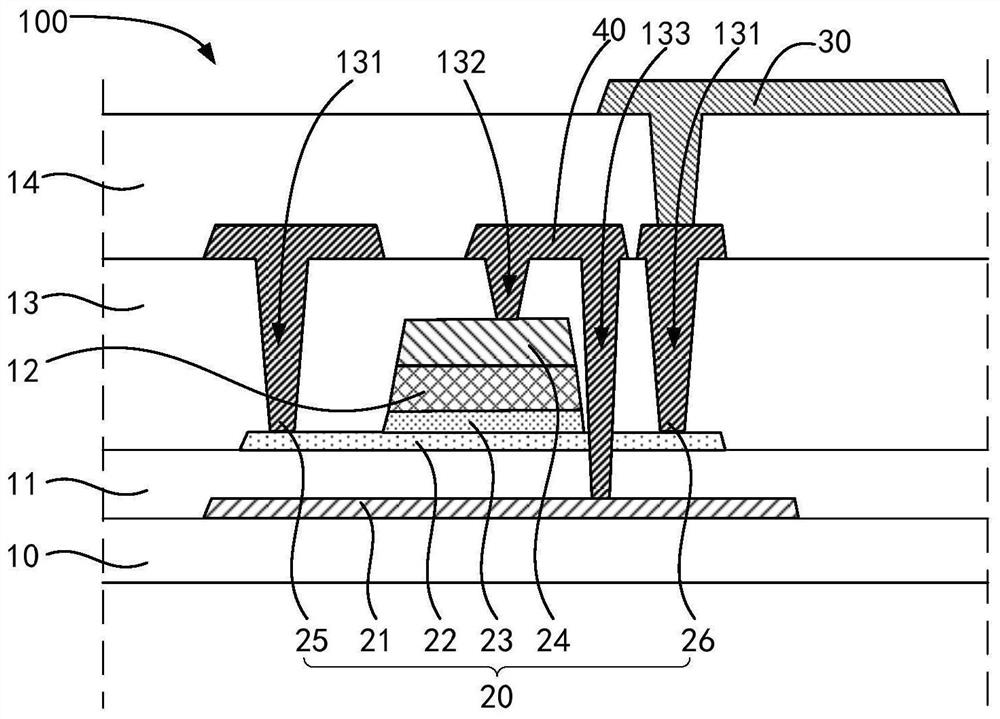
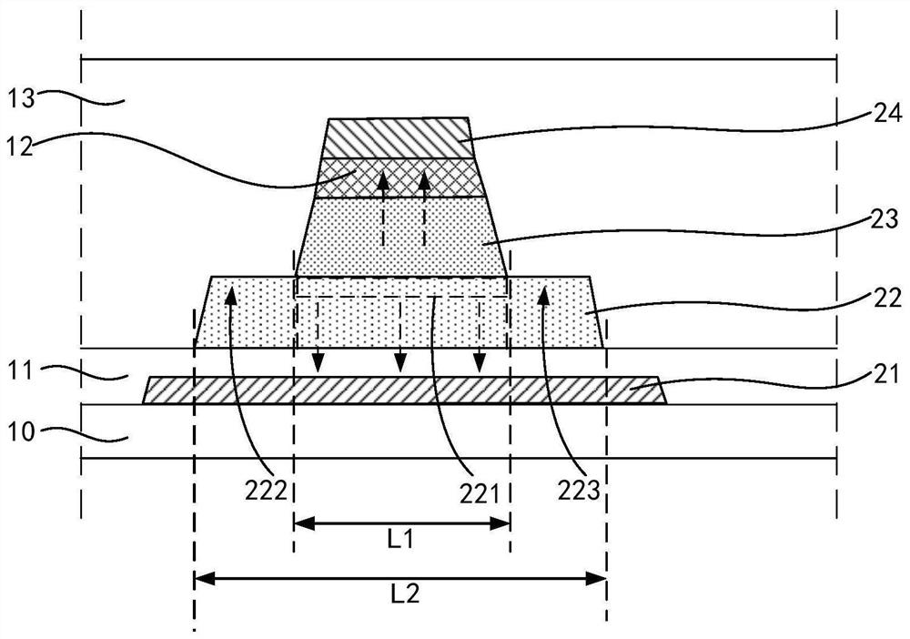
[0038] The following descriptions of the various embodiments refer to the accompanying drawings to illustrate specific embodiments that the present application can be used to implement. The directional terms mentioned in this application, such as [top], [bottom], [front], [back], [left], [right], [inside], [outside], [side], etc., are for reference only The orientation of the attached schema. Therefore, the directional terms used are used to illustrate and understand the application, but not to limit the application. In the figures, structurally similar elements are denoted by the same reference numerals. In the drawings, the thicknesses of some layers and regions are exaggerated for clear understanding and ease of description. That is, the size and thickness of each component shown in the drawings are arbitrarily shown, but the present application is not limited thereto.

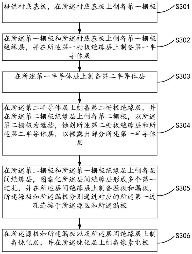
[0039] Aiming at the problem of poor light stability of the existing oxide semiconductor thin film tr...


PUM


Abstract

The invention provides an array substrate, a preparation method thereof and a display panel. The array substrate comprises a substrate body and a thin film transistor arranged on the substrate body, and the thin film transistor comprises a first grid electrode, a first semiconductor layer, a second semiconductor layer, a second grid electrode, a source electrode and a drain electrode which are sequentially arranged on the substrate body. A conducting channel of the thin film transistor is formed on the contact surface of a first semiconductor layer and a second semiconductor layer, and the conducting channel is formed between the semiconductor layers made of the same material, so that an interface defect state caused by material difference when the existing conducting channel is formed on one side, close to an insulating layer, of the semiconductor layer can be avoided; therefore, the problem of poor illumination stability of the existing oxide semiconductor thin film transistor is solved.

Description

technical field [0001] The present application relates to the field of display technology, in particular to an array substrate, a manufacturing method thereof, and a display panel. Background technique [0002] In the active matrix display technology, each sub-pixel is driven by a thin film transistor (Thin Film Transistor, TFT) integrated thereon, so that high-speed, high-brightness, and high-contrast screen display effects can be achieved. Thin film transistors are mainly divided into amorphous silicon (a-Si) thin film transistors, low temperature polysilicon (LowTemperature Poly-silicon, LTPS) thin film transistors and oxide semiconductor (Oxide semiconductor) thin film transistors according to the material of the semiconductor layer, and oxide semiconductor thin film transistors ( Oxide TFT) has been widely used due to its simpler manufacturing process compared with low-temperature polysilicon thin film transistors and higher compatibility with amorphous silicon thin fil...

Claims


Application Information

Patent Timeline
IPC IPC(8): H01L27/12H01L21/77
CPCH01L27/1222H01L27/1225H01L27/127H01L29/78696H01L29/7869H01L29/78648
Inventor 黄旭
Owner HUIZHOU CHINA STAR OPTOELECTRONICS TECHNOLOGY CO LTD
Features
  • R&D
  • Intellectual Property
  • Life Sciences
  • Materials
  • Tech Scout
  • Unparalleled Data Quality
  • Higher Quality Content
  • 60% Fewer Hallucinations
Learn More