Ka-band wide-stop-band filtering power divider

A technology of wide stop band and power divider, applied in the field of communication, to achieve the effect of excellent out-of-band suppression characteristics

Active Publication Date: 2022-03-11
西安电子科技大学重庆集成电路创新研究院
View PDF8 Cites 2 Cited by
  • Summary
  • Abstract
  • Description
  • Claims
  • Application Information

AI Technical Summary

Problems solved by technology

[0006]At present, there is a technical gap in the Ka-band wide stopband filter power splitter that uses SIW technology to achieve good out-of-band suppression effect

Method used


Image

  • Ka-band wide-stop-band filtering power divider
  • Ka-band wide-stop-band filtering power divider
  • Ka-band wide-stop-band filtering power divider

Examples


Embodiment 1

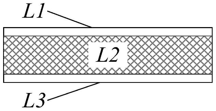
[0052] See figure 1 , figure 1 A schematic structural diagram of a Ka-band wide stopband filter power divider provided by an embodiment of the present invention. The filter power divider includes a first metal layer L1, a dielectric layer L2 and a second metal layer L3 stacked in sequence. Specifically, the first metal layer L1 , the dielectric layer L2 and the second metal layer L3 are arranged sequentially from top to bottom.

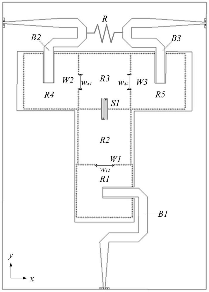
[0053] See figure 2 , figure 2 A top view of the first metal layer and dielectric layer of a filter power splitter provided by an embodiment of the present invention.

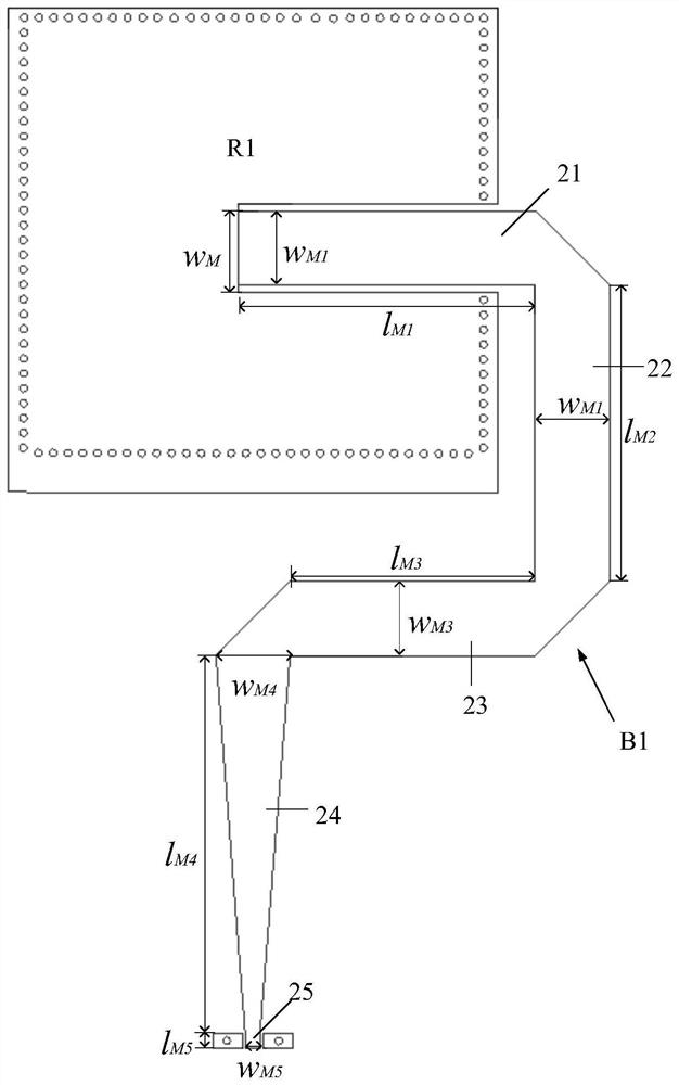
[0054] An input coupling line B1 , a first output coupling line B2 and a second output coupling line B3 are disposed on the sidewall of the first metal layer L1 , and an S-shaped groove S1 is opened in the middle of the first metal layer L1 . The dielectric layer L2 runs through a plurality of conductor columns, and the plurality of conductor columns form a first resonant cavity...

Embodiment 2

[0086] See Figure 10 , Figure 10 A schematic structural diagram of another Ka-band wide stop-band filter power divider provided by an embodiment of the present invention. The filter power divider includes a first metal layer L1, a dielectric layer L2 and a second metal layer L3 stacked in sequence. Specifically, the first metal layer L1 , the dielectric layer L2 and the second metal layer L3 are arranged sequentially from top to bottom.

[0087] See Figure 11 , Figure 11 A top view of the first metal layer and the dielectric layer of another filter power splitter provided by an embodiment of the present invention.

[0088] An input coupling line B1 , a first output coupling line B2 and a second output coupling line B3 are disposed on the sidewall of the first metal layer L1 , and an S-shaped groove S1 is opened in the middle of the first metal layer L1 . The dielectric layer L2 runs through a plurality of conductor columns, and the plurality of conductor columns form ...


PUM


Abstract

The Ka-band wide-stop-band filtering power divider comprises a first metal layer, a dielectric layer and a second metal layer which are stacked in sequence, an input coupling line, a first output coupling line and a second output coupling line are arranged on the side wall of the first metal layer, and an S-shaped groove is formed in the middle of the first metal layer; a plurality of conductor columns penetrate through the dielectric layer, and the conductor columns, the first metal layer and the second metal layer form a first resonant cavity, a second resonant cavity, a third resonant cavity, a fourth resonant cavity and a fifth resonant cavity. An input coupling line and an output coupling line of the filtering power divider extend into the resonant cavities, electrical coupling is realized by adopting an input and output deep feeder line structure, and the input coupling line and the output coupling line form a reasonable coupling matrix of the filter together with electrical coupling realized between the second resonant cavity and the third resonant cavity by utilizing an S-shaped groove structure; and effective suppression of coupling between high-order mode cavities is realized by using the distribution characteristics of each parasitic electromagnetic mode, and the excellent out-of-band suppression characteristic of the filtering power divider is realized.

Description

technical field [0001] The invention belongs to the technical field of communication, and in particular relates to a Ka-band wide stopband filter power divider. Background technique [0002] With the continuous development of semiconductor technology, high-performance integrated passive devices (integrated passive devices, IPDs) based on through-silicon vias (Through Silicon Via, TSV) have gradually been widely used. The TSV-based IPD has good performance and miniaturization characteristics, which can improve the performance of the entire integrated radar system and communication system. However, the high cost and high loss of silicon-based interposers limit their market application. Based on this, through glass via (through glass via, TGV) has become a research hotspot in the current three-dimensional interconnection materials due to its excellent electrical properties and low loss. [0003] Compared with silicon substrates, glass substrates have excellent high-frequency ...

Claims


Application Information

Patent Timeline
Patent Type & Authority Applications(China)
IPC IPC(8): H01P5/16
CPCH01P5/16
Inventor 刘晓贤范晨晖朱樟明刘诺张涛刘阳卢启军
Owner 西安电子科技大学重庆集成电路创新研究院
Why Eureka
Try Eureka