
Circuit board tape and butt joint method thereof

A circuit and board roll technology, applied in the directions of printed circuit, printed circuit, printed circuit manufacturing, etc., can solve the problems of inability to carry out the process, the variation of the transmission hole distance, etc., and achieve the effect of the number of circuit layouts

Pending Publication Date: 2022-03-11
CHIPBOND TECH
View PDF0 Cites 0 Cited by
  • Summary
  • Abstract
  • Description
  • Claims
  • Application Information

AI Technical Summary

Problems solved by technology

[0004] The main purpose of the present invention is to increase the number of circuit layouts without changing the hole spacing between the drive holes and the length of the circuit board tape; Maintain the arrangement at equal intervals to solve the problem in the prior art that the subsequent process cannot be performed due to the variation in the distance between the jointed transmission holes caused by the operator's indeterminate cutting position

Method used


Image

  • Circuit board tape and butt joint method thereof
  • Circuit board tape and butt joint method thereof
  • Circuit board tape and butt joint method thereof

Examples


Embodiment Construction

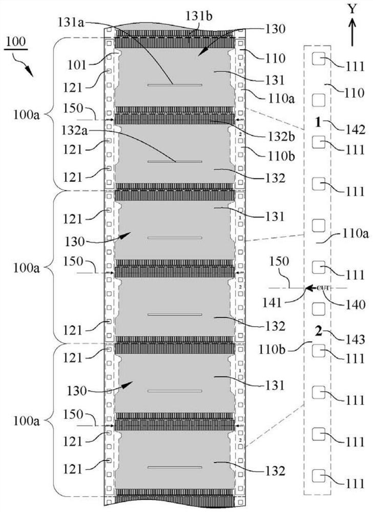
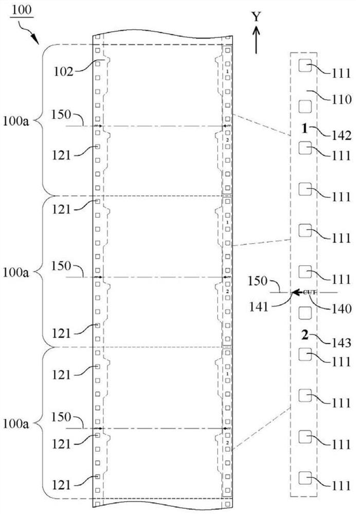
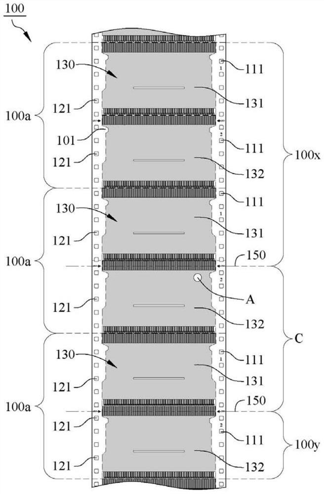
[0044] see figure 1 and figure 2, a circuit board tape 100 of the present invention has a first surface 101 and a second surface 102, the circuit board tape 100 includes a plurality of substrate units 100a arranged along the transmission direction Y, each of the substrate units 100a has a first A transmission hole setting area 110, a second transmission hole setting area 120, a circuit layout area 130 and at least one docking mark 140, the first transmission hole setting area 110 has more than three first transmission holes 111 with an odd number, so The first transmission holes 111 are equidistantly arranged on one side of the substrate unit 100a, please refer to figure 1 and figure 2 In the partial enlarged view, in this embodiment, the first transmission hole setting area 110 has 11 first transmission holes 111 for illustration, but it is not limited thereto.

[0045] see figure 1 and figure 2 , the second transmission hole setting area 120 has more than three secon...


PUM


Abstract

The invention relates to a circuit board tape and a butt joint method thereof. The circuit board tape comprises a plurality of substrate units, each substrate unit is provided with a transmission hole setting area, a circuit layout area and a butt joint mark, the transmission hole setting area is provided with more than three transmission holes, the number of the transmission holes is an odd number, the circuit layout area is provided with a first circuit layout and a second circuit layout, and the butt joint mark extends to form a virtual line. The virtual lines are located between the first circuit layout and the second circuit layout, an odd number of transmission holes are formed between the virtual lines of the adjacent substrate units, and the unqualified substrate units are cut off along the virtual lines of the different substrate units, so that the circuit board winding tape is broken into a front winding tape part and a rear winding tape part; and after the front winding tape part and the rear winding tape part are jointed, a first circuit layout arranged on the front winding tape part and a second circuit layout arranged on the rear winding tape part form a composite circuit layout area.

Description

technical field [0001] The invention relates to a circuit board tape and its docking method, in particular to a circuit board tape that can be docked after cutting unqualified substrate units and its docking method. Background technique [0002] In the existing known circuit board tape design, a plurality of circuit layouts are arranged on the substrate, and a plurality of transmission holes are provided on both sides of the substrate, and each of the two sides of the circuit layout corresponds to an even number of transmission holes. And the pitch between the transmission holes must match the tooth pitch of the transmission member (such as a transmission wheel or a transmission bar), so that the transmission member can drive the substrate to carry out processes such as bonding wafers and gluing. [0003] However, in the inspection step, the area with the unacceptable circuit layout is cut off, so that the circuit board reel is formed into a front reel and a rear reel, and t...

Claims


Application Information

Patent Timeline
Patent Type & Authority Applications(China)
IPC IPC(8): H05K1/02H05K3/00H05K3/40
CPCH05K1/028H05K1/0266H05K1/0296H05K3/00H05K3/40H05K2201/09H05K2203/166H05K13/0084H05K13/0061H05K13/0419H05K2201/09936H05K2203/1545H05K2203/0228H05K2201/09063H05K1/189H05K3/368H05K1/0269H05K3/0052H05K1/0393H05K13/0215
Inventor 林吟贞柯明孝黄惠愈彭智明李俊德
Owner CHIPBOND TECH
Learn More