Insulator defect detection method based on machine learning
A defect detection and machine learning technology, applied in neural learning methods, optical testing flaws/defects, instruments, etc., can solve problems such as low recognition rate, high photo requirements, and inability to completely solve lighting problems, achieving high recognition rate and training. Sample low effect
- Summary
- Abstract
- Description
- Claims
- Application Information
AI Technical Summary
Problems solved by technology
Method used
Image
Examples
Embodiment Construction
[0044] The present invention will be further described in detail through the drawings and examples below. Through these descriptions, the features and advantages of the present invention will become more apparent.
[0045] The word "exemplary" is used exclusively herein to mean "serving as an example, embodiment, or illustration." Any embodiment described herein as "exemplary" is not necessarily to be construed as superior or better than other embodiments. While various aspects of the embodiments are shown in drawings, the drawings are not necessarily drawn to scale unless specifically indicated.
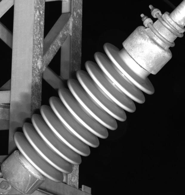
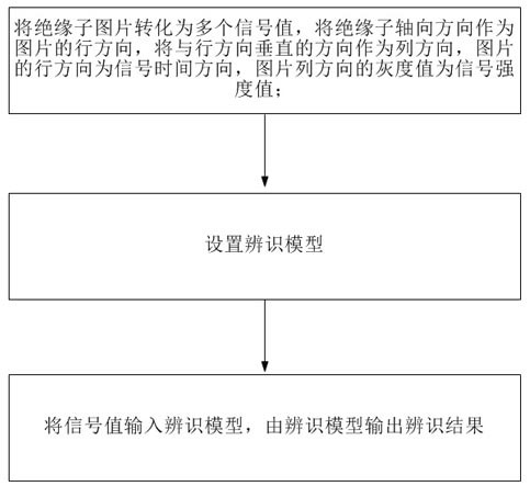
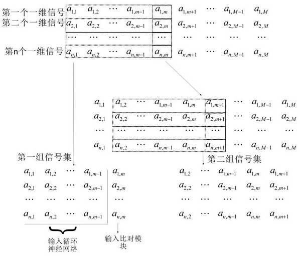
[0046] On the one hand, the present invention proposes an insulator defect detection method based on machine learning. According to the characteristics of insulators, the brightness value of the insulator in the picture is extracted, the brightness value is converted into a signal value, and the signal value is input to the neural network to obtain Detection results of insulator d...
PUM
 Abstract
Description
Claims
Application Information


