Wafer supporting seat and process cavity

A support seat and wafer technology, applied in the direction of discharge tubes, electrical components, circuits, etc., can solve problems such as difficult duplication of circuit components and affecting radio frequency transmission

Pending Publication Date: 2022-03-18
PIOTECH CO LTD
View PDF1 Cites 0 Cited by
  • Summary
  • Abstract
  • Description
  • Claims
  • Application Information

AI Technical Summary

Problems solved by technology

The disadvantage of such a configuration is that it is necessary to additionally connect the radio frequency adjustment circuit to the cavity (changing the impedance through a variable capacitor), and it is only suitable for wafer support plates made of ceramics.
Due to the external connection of the RF adjustment circuit, the relatively long circuit loop accumulates a certain inductive impedance, which affects the RF transmission
Furthermore, such a configuration may be difficult to reproduce in different stations or chambers due to slight differences in circuit components, but at the same time require these stations and chambers to perform the same process

Method used


Image

  • Wafer supporting seat and process cavity
  • Wafer supporting seat and process cavity
  • Wafer supporting seat and process cavity

Examples


Embodiment Construction

[0030] The present invention will now be described more fully hereinafter with reference to the accompanying drawings, in which certain exemplary embodiments are shown by way of illustration. However, claimed subject matter may be embodied in many different forms, and thus constructions of covered or claimed subject matter are not limited to any example embodiments disclosed in this specification; the example embodiments are merely illustrations. Likewise, the invention resides in providing a reasonably broad scope for claimed subject matter as claimed or covered.

[0031] The term "in one embodiment" used in this specification does not necessarily refer to the same embodiment, and the use of "in other (some / some) embodiments" in this specification does not necessarily refer to different embodiments. It is intended, for example, that claimed subject matter includes combinations of all or some of the exemplified embodiments.

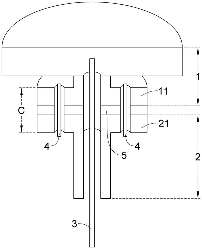
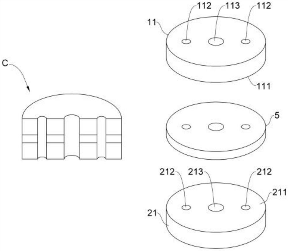
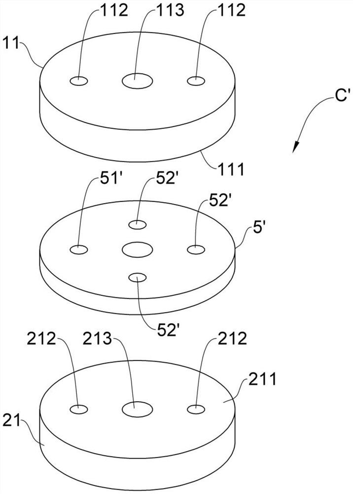
[0032] figure 1 The wafer support seat of the pre...


PUM


Abstract

The invention discloses a wafer supporting seat, which comprises a supporting disc, a first connecting part and a second connecting part, the shaft is provided with a top end and a second connecting part located at the top end, and the second connecting part is detachably connected with the first connecting part, so that the top end of the shaft is detachably connected to the bottom of the supporting disc; and the insulating medium sheet is clamped between the first connecting part of the supporting disc and the second connecting part of the shaft, so that a capacitor in the electrode loop is formed. In addition, the invention also discloses a process cavity.

Description

technical field [0001] The invention relates to a semiconductor device, in particular to a wafer support seat and a process chamber. Background technique [0002] In semiconductor manufacturing, plasma processing is commonly used for deposition or etching. Plasma treatment has more advantages than general heat treatment, for example, plasma enhanced chemical vapor deposition (PECVD) allows deposition to be achieved at relatively low temperatures and to achieve higher deposition rates. The current challenge of PECVD is the uniformity of the plasma in the chamber, and the uniformity of the thickness of the deposited film at the center and edge of the wafer. [0003] Various prior art techniques are known to propose means to improve the distribution of the plasma within the cavity. U.S. Patent Publication No. US20200010957A1 discloses an improvement method starting from the electrode circuit, which includes electrically connecting the lower electrode in the wafer support plat...

Claims


Application Information

Patent Timeline
Patent Type & Authority Applications(China)
IPC IPC(8): H01J37/32
CPCH01J37/32715H01J37/32458H01J37/32082H01J2237/3321
Inventor 张赛谦
Owner PIOTECH CO LTD
Why Eureka
Try Eureka