Transfer device and transfer method of micro light-emitting diode
A technology of light-emitting diodes and transfer devices, which is applied in the manufacture of electrical components, electric solid-state devices, semiconductor/solid-state devices, etc. It can solve the problems of easy breakage and fragility of the bridge arm structure, and small micro-light-emitting diodes, so as to ensure the success rate of transfer , Reduce environmental pollution, high transfer success rate
- Summary
- Abstract
- Description
- Claims
- Application Information
AI Technical Summary
Problems solved by technology
Method used
Image

Examples
Embodiment 1
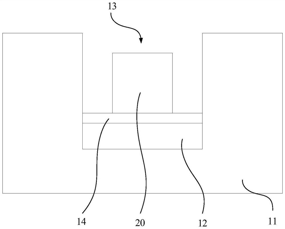
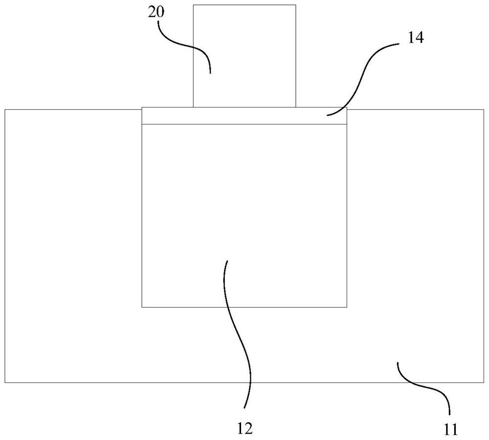
[0029] refer to Figure 1 ~ Figure 4 , the present invention discloses a transfer device for micro light emitting diodes 20, comprising: a carrier substrate 11 and an expandable material 12, the carrier substrate 11 is provided with a groove 13 for accommodating the micro light emitting diodes 20, the expandable material 12 is arranged in the concave Bottom of tank 13. By disposing the expandable material 12 at the bottom of the groove 13, the groove 13 is used to accommodate the micro LED 20, the groove 13 can protect the micro LED 20 and reduce environmental pollution, when the micro LED 20 needs to be transferred to the target substrate At this time, it is only necessary to stimulate the expansion of the expandable material 12, and the expansion of the expandable material 12 will push the micro light emitting diodes 20 out of the groove 13, so that the micro light emitting diodes 20 can be combined with the target substrate, and the expandable material 12 can make all the m...
Embodiment 2
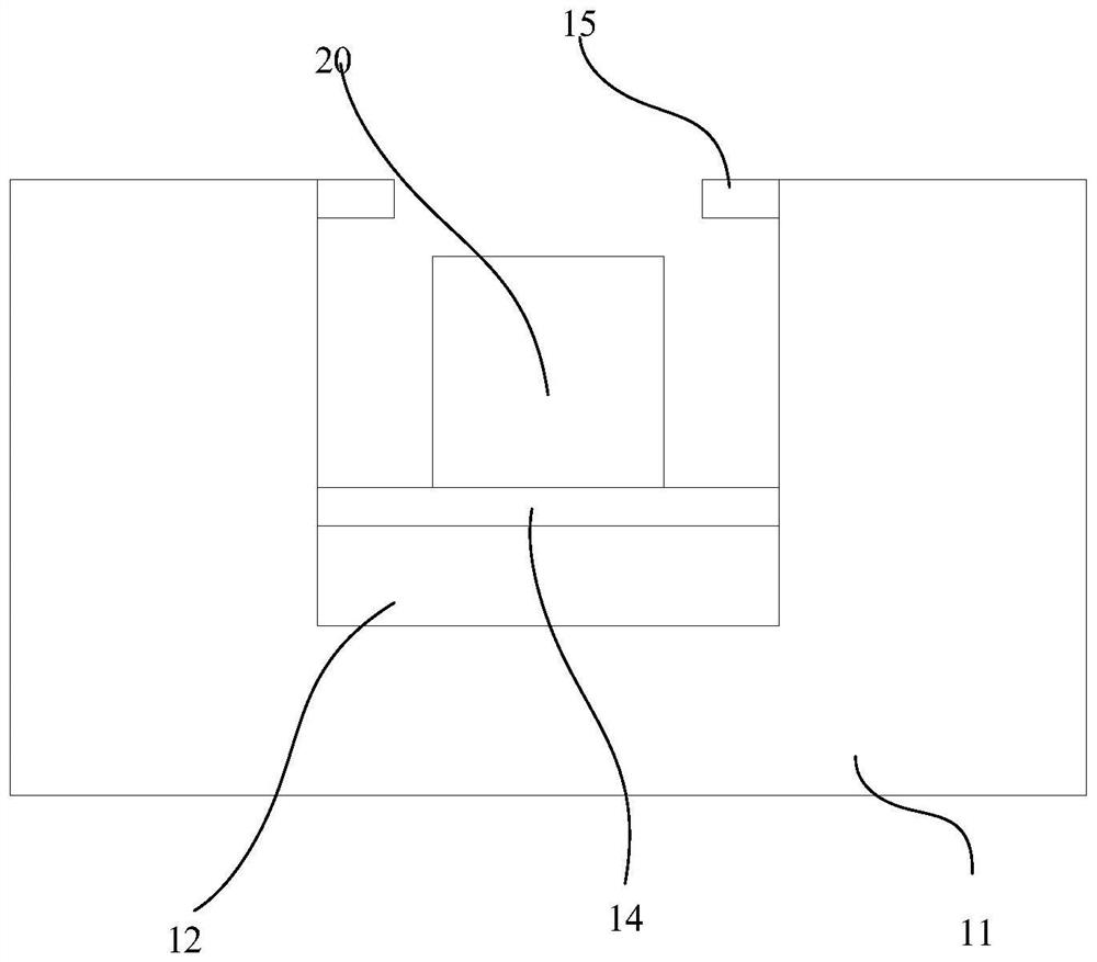
[0061] refer to Figure 5 to Figure 9 Compared with Embodiment 1, the improvement of Embodiment 2 is that the transfer device also includes a positioning structure arranged on the carrier substrate 11, and the positioning structure is used to position the micro-LEDs 20 so that the micro-LEDs 20 are directly opposite to the transfer device. , especially when there are multiple micro light emitting diodes 20, the positioning structure can position all micro light emitting diodes 20 at once. By setting the positioning structure, it can facilitate the positioning with the batch of micro light emitting diodes 20 , and reduce the difficulty of positioning the transfer device with the batch of micro light emitting diodes 20 .
[0062] refer to Figure 5 with Figure 7 , in a specific embodiment, the positioning structure is a snapping structure 16, the array substrate includes a base 25 and a plurality of micro light emitting diodes 20 distributed on the base 25 in an array, the sn...
Embodiment 3
[0091] Compared with Embodiment 1 and Embodiment 2, the improvement of Embodiment 3 is the further improvement of the material of the carrier substrate 11 .
[0092] In a specific embodiment, the reference figure carrier substrate 11 includes a bottom plate 111 and a top plate 112 connected to the bottom plate 111, the top plate 112 is provided with a groove 13, and the material of the top plate 112 is a flexible resin material (polyimide, epoxy resin etc.), eutectic metal or soft metal and other flexible materials, the groove 13 can be formed by grinding, embossing or etching the top plate 112 . The purpose of setting the top plate 112 on the above-mentioned flexible material is to make the top plate 112 easy to bond with the temporary transfer substrate or substrate through pressure, so that the top plate 112 is fixedly connected with the temporary transfer substrate or substrate, and the coating and adhesive can be omitted. agent steps, making the process simpler.
[0093]...
PUM
 Abstract
Description
Claims
Application Information
 - R&D Engineer
- R&D Manager
- IP Professional
- Industry Leading Data Capabilities
- Powerful AI technology
- Patent DNA Extraction
Browse by: Latest US Patents, China's latest patents, Technical Efficacy Thesaurus, Application Domain, Technology Topic.
© 2024 PatSnap. All rights reserved.Legal|Privacy policy|Modern Slavery Act Transparency Statement|Sitemap