Optical imaging system

An optical imaging system and optical technology, applied in optics, instruments, photography, etc., can solve the problems of inability to brighten the outer surface of semiconductor chips, shadows in images, etc., to avoid blind spots or uneven brightness, and improve imaging quality. Effect

Pending Publication Date: 2022-03-22
深圳市华拓半导体技术有限公司
View PDF0 Cites 0 Cited by
  • Summary
  • Abstract
  • Description
  • Claims
  • Application Information

AI Technical Summary

Problems solved by technology

[0006] In view of the shortcomings of the above-mentioned prior art, the purpose of the present invention is to provide an optical imaging system, which aims to solve the problem that the existing light source cannot fully illuminate the outer surface of the semiconductor chip when the semiconductor chip is photographed by the photographing device. , resulting in the problem of shadows in the captured image

Method used


Image

  • Optical imaging system
  • Optical imaging system
  • Optical imaging system

Examples


Embodiment

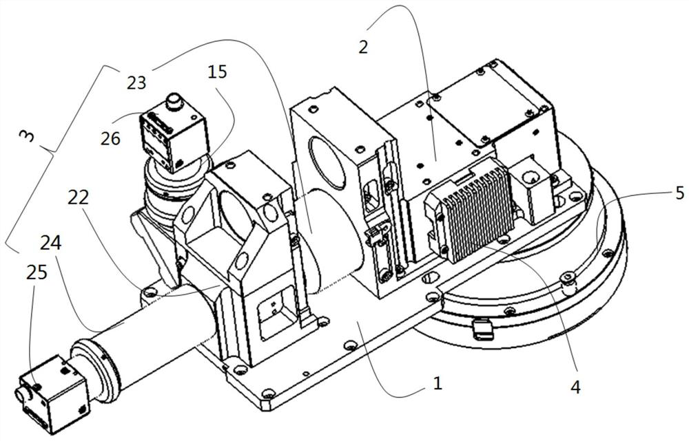
[0056] The invention discloses an optical imaging system, please refer to figure 1 , figure 1 It is a schematic diagram of the first structure of an optical imaging system provided by the present invention. The embodiment of the present invention includes an optical main panel 1, an optical module 2, a camera module 3, a side coaxial light source module 4 and a multi-angle light source module 5; wherein, the optical main panel 1 is a common plate-shaped structure, on which Several connecting holes are provided for connecting with each module to support each module. The optical module 2 and the camera module 3 are both arranged on the surface of the optical main plate 1, and the camera module 3 is set towards the refracted light direction of the optical module 2, the optical module 2 is used to transmit the reflected light of the measured object to the camera module 3, and the camera module 3 is set on the optical path of the characteristic imaging light of the measured object...


PUM


Abstract

The invention discloses an optical imaging system which comprises an optical main flat plate, an optical module, a camera module, a side edge coaxial light source module and a multi-angle light source module. Wherein the optical module and the camera module are both arranged on the surface of the optical main flat plate, and the camera module is arranged towards the refracted light direction of the optical module; the side edge coaxial light source module is arranged on the side face of the optical module, and the light emitting direction of the side edge coaxial light source module faces the optical module. The multi-angle light source module is arranged on the surface, deviating from the optical module, of the optical main flat plate, and the multi-angle light source module is communicated with the optical module; the light emitting direction of the multi-angle light source module deviates from the optical module. The optical path of the light emitted by the side coaxial light source module is adjusted to be emitted from the side of the measured object to the measured object through the optical module, and the multi-angle light source module surrounds the measured object, so that the situation of light blind areas or non-uniform brightness during lighting is avoided, the measured object is lighted in all directions, and the imaging quality is improved.

Description

technical field [0001] The invention relates to the technical field of optical imaging, in particular to an optical imaging system. Background technique [0002] Semiconductor chips refer to electronic components whose conductivity is between conductors and insulators at room temperature. With the development of electronic component packaging in the direction of miniaturization and high integration, correspondingly, semiconductor chips are also gradually tending to miniaturization production. [0003] In the manufacturing process of semiconductor chips, it is necessary to detect whether there are crystal defects in the finished product. The traditional way is to observe the surface of the chip visually. Due to the huge market demand, the production volume has also doubled. Generally, there are hundreds of chips on a piece of material, which are small in size and dense in arrangement. It takes a lot of time to detect chips with human eyes, and it is easy to miss and misre...

Claims


Application Information

Patent Timeline
IPC IPC(8): G03B15/02G03B15/03G03B15/06
CPCG03B15/02G03B15/03G03B15/06
Inventor 罗建华师晓科刘佳华何李超邓小云
Owner 深圳市华拓半导体技术有限公司
Why Eureka
Try Eureka