Device for improving error of digital controllable attenuation semiconductor chip

A semiconductor and control device technology, which is applied in the direction of impedance network, electrical components, multi-terminal pair network, etc., can solve the problem of increasing attenuation error, achieve the effect of reducing attenuation error, improving isolation, and ensuring accuracy and stability

Pending Publication Date: 2022-04-01
南京元络芯科技有限公司
View PDF0 Cites 2 Cited by
  • Summary
  • Abstract
  • Description
  • Claims
  • Application Information

AI Technical Summary

Problems solved by technology

like image 3 and Figure 4 As shown, taking 24dB attenuation as an example, the simulation results consistent with the above analysis can be obtained. In 0-10GHz, the attenuation value will change by about 4dB, and the trend is opposite to the frequency change in the straight-through state, resulting in relative attenuation further increase in error

Method used


Image

  • Device for improving error of digital controllable attenuation semiconductor chip
  • Device for improving error of digital controllable attenuation semiconductor chip
  • Device for improving error of digital controllable attenuation semiconductor chip

Examples


Embodiment 1

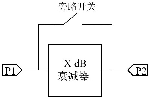
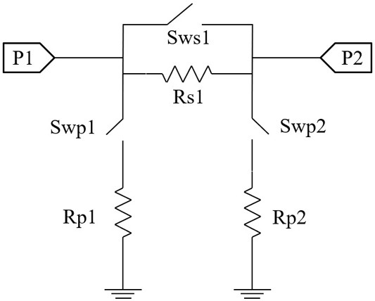
[0035] The present embodiment provides a device for improving digital controllable attenuation of semiconductor chip errors, such as Figure 5 and Figure 11 As shown, it includes a bypass series switch group and a regulating device, the bypass series switch group and the digital controllable attenuator are arranged in parallel at the electrical node between the port P1 and the port P2, and the bypass series switch group has a symmetrical circuit structure, One end of the control device is connected to the electrical node of the symmetrical center of the bypass switch group, and the other end is grounded. The device is connected in parallel with the bypass series switch group on the attenuator, and is grounded through the control device, which can effectively improve the connection between port P1 and port P2. The isolation in the attenuation state reduces the attenuation error and ensures the accuracy and stability of the relative attenuation of the digital controllable atten...

Embodiment 2

[0041] According to the device for improving digitally controllable attenuation semiconductor chip errors described in Embodiment 1, the π-type digitally controllable attenuator is replaced by a T-type digitally controllable attenuator.

[0042] Beneficial effects of the present invention:

[0043] In the present invention, a digitally controllable attenuator is connected in parallel with a bypass series switch group that can be grounded, which can effectively increase the isolation between the port P1 and the port P2, and significantly reduce the attenuation value error caused by insufficient isolation, thereby largely Ensure relative attenuation accuracy.

[0044] Those skilled in the art should understand that the embodiments of the present application may be provided as methods, systems, or computer program products. Accordingly, the present application may take the form of an entirely hardware embodiment, an entirely software embodiment, or an embodiment combining softwa...


PUM


Abstract

The invention discloses a device for improving errors of a digital controllable attenuation semiconductor chip, which comprises a bypass series switch group and a regulation and control device, and is characterized in that the bypass series switch group and a digital controllable attenuator are arranged in parallel at an electric node between a port P1 and a port P2; the bypass series switch group is connected with the regulation and control device and then is grounded. The regulation and control device is used for improving the isolation degree between the port P1 and the port P2 in the attenuation state. According to the device, the grounded bypass series switch group is connected in parallel on the attenuator, so that the isolation degree of the port P1 and the port P2 in the attenuation state can be effectively improved, the attenuation error is reduced, and the accuracy and the stability of relative attenuation in the straight-through state and the attenuation state are ensured.

Description

technical field [0001] The invention relates to a device for improving the error of a digital controllable attenuation semiconductor chip, which belongs to the technical field of controllable attenuators. Background technique [0002] The internal core of the digital controllable attenuator designed based on semiconductor technology is a digital controllable attenuation semiconductor chip, and the circuit integration of the digital controllable attenuator is arranged in the semiconductor chip. [0003] Digital controllable attenuators usually use the different states of each switch to switch between the attenuation state and the through state. Its structure types mainly include π-type and T-type, and its functional structure is as follows: figure 1 shown. [0004] Taking the π-type structure as an example, such as figure 2 As shown, in the straight-through state, the switch Sws1 is ON, the switch Swp1 is OFF, and the switch Swp2 is OFF, the switch Sws1 is equivalent to a ...

Claims


Application Information

Patent Timeline
Patent Type & Authority Applications(China)
IPC IPC(8): H03H7/24
Inventor 孙志远王静波
Owner 南京元络芯科技有限公司
Why Eureka
Try Eureka