Circuit and method for modifying chip system memory for burning

A chip system and memory technology, which is applied in the circuit field of modifying the memory of the chip system for burning, can solve the problem that the user cannot modify the content, etc., and achieve the effect of convenient debugging and testing

Pending Publication Date: 2022-04-12
苏州洪芯集成电路有限公司
View PDF0 Cites 1 Cited by
  • Summary
  • Abstract
  • Description
  • Claims
  • Application Information

AI Technical Summary

Problems solved by technology

The system memory can usually only be written to when the chip is manufactured, and the user cannot modify the content

Method used


Image

  • Circuit and method for modifying chip system memory for burning
  • Circuit and method for modifying chip system memory for burning
  • Circuit and method for modifying chip system memory for burning

Examples


Embodiment Construction

[0023] In order to further understand the invention content, features and effects of the present invention, the detailed description is as follows in conjunction with the accompanying drawings.

[0024] Please also refer to Figure 1 to Figure 5 In the following, a circuit and method for modifying system-on-chip memory for programming according to the present invention will be described in detail in conjunction with the accompanying drawings.

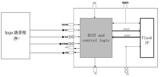
[0025] Such as figure 1 As shown, a circuit for modifying the on-chip system memory for programming by means of the flash bist test mechanism of the present invention includes FPGA, MCU test board, chip to be tested, downloader and host computer, and the chip to be tested is installed on the MCU test board Connect the flash to the corresponding pins of the MCU test board, connect the power supply pins of the FPGA and MCU test board to the power supply, ground the GND pin of the FPGA and MCU test board, connect one end of the downloader...


PUM


Abstract

The invention discloses a circuit and a method for modifying a chip system memory for burning. The method comprises the following steps: (1) writing an FPGA (Field Programmable Gate Array) project file; (2) burning the project file into an FPGA (Field Programmable Gate Array); (3) completing circuit connection; (4) starting to burn the program, and outputting a control instruction to the flash by the engineering file by means of bist pad so as to modify the data of the system memory; and (5) detecting whether the program is burnt successfully or not. According to the method, the bist test pad of the flash in the chip is utilized to enter the bist mode, the chip to be tested is connected through the fpga board, the corresponding erasing instruction and content are sent to the bist serial interface, the content of a system memory can be modified after the chip leaves a factory, a BootLoader program can be conveniently tested, and the chip can conveniently debug and test the flash.

Description

technical field [0001] The invention relates to a circuit and method for modifying a memory of a chip system for programming and belongs to the technical field of chip testing. Background technique [0002] Flash is a kind of memory chip, and the data inside can be modified through a specific program. Flash often means Flash Memory in the field of electronics and semiconductors, which is usually called "flash memory". Flash memory, also known as flash memory, combines the strengths of ROM and RAM. It not only has the performance of electronically erasable and programmable (EEPROM), but also can read data quickly (the advantage of NVRAM), so that data will not be lost due to power failure. . [0003] Flash has 3 startup modes, one of which is to start with BootLoader in system memory (system memory). The system memory contains the BootLoader program, which can be used to reprogram the flash memory using the USART1 serial interface. The system memory can usually only be wr...

Claims


Application Information

Patent Timeline
Patent Type & Authority Applications(China)
IPC IPC(8): G06F8/61
Inventor 张旭徐建华
Owner 苏州洪芯集成电路有限公司
Why Eureka
Try Eureka