Sample transmission device and semiconductor equipment

A sample transmission and semiconductor technology, which is applied in the field of sample transmission devices and semiconductor equipment, can solve problems such as transmission table collisions, and achieve the effect of eliminating collisions

Pending Publication Date: 2022-04-12
SHANGHAI PRECISION MEASUREMENT SEMICON TECH INC
View PDF0 Cites 0 Cited by
  • Summary
  • Abstract
  • Description
  • Claims
  • Application Information

AI Technical Summary

Problems solved by technology

[0005] The purpose of the present invention is to disclose a sample transmission device and a semiconductor device based on the sample transmission device, so as to solve the problem of collision of transmission tables in the prior art

Method used


Image

  • Sample transmission device and semiconductor equipment
  • Sample transmission device and semiconductor equipment
  • Sample transmission device and semiconductor equipment

Examples


Embodiment Construction

[0025] The present invention will be described in detail below in conjunction with the implementations shown in the drawings, but it should be noted that these implementations are not limitations of the present invention, and those of ordinary skill in the art based on the functions, methods, or structural changes made by these implementations Equivalent transformations or substitutions all fall within the protection scope of the present invention.

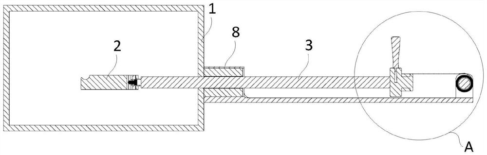
[0026] Such as Figure 1-4 As shown, the present embodiment provides a sample transfer device for transferring samples (such as wafers) in the cavity 1 of the semiconductor device, including:

[0027] Transfer table 2 for placing samples;

[0028] A transfer rod 3, used to push and pull the transfer table 2 to transfer samples in the cavity 1;

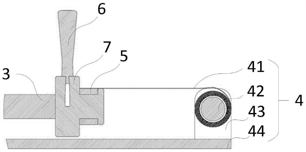
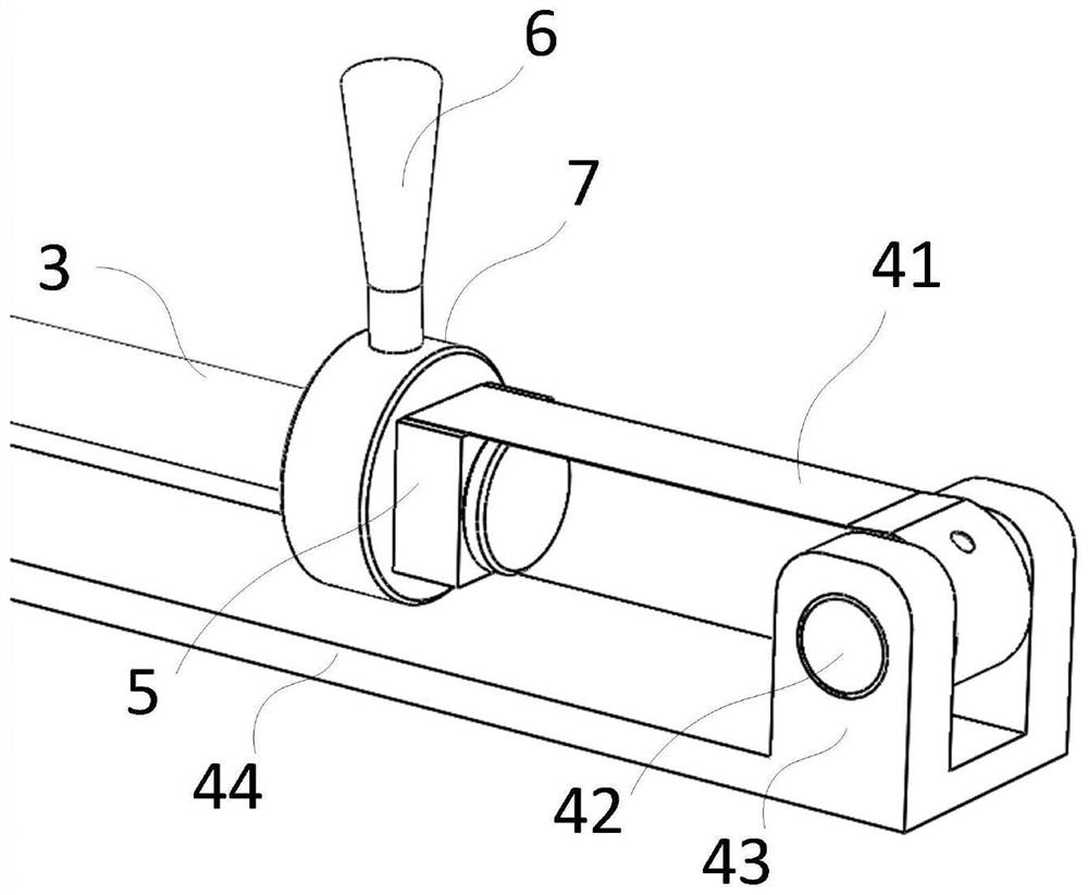
[0029] A constant force component 4 , one end of the constant force component 4 is connected to the transmission rod 3 , and the constant force component 4 exerts a constant pulling forc...


PUM


Abstract

The invention discloses a sample transmission device, which is used for transmitting a sample in a cavity of semiconductor equipment, and comprises a transmission table for placing the sample; the conveying rod is used for pushing and pulling the conveying table so as to convey the sample in the cavity; and one end of the constant force assembly is connected with the conveying rod, and the constant force assembly applies constant pulling force to the conveying rod. The invention also discloses semiconductor equipment which comprises a cavity and the sample transmission device. According to the sample transmission device and the semiconductor equipment provided by the invention, the constant force assembly is used for providing the constant pulling force for the transmission rod, so that the standing transmission rod and the transmission table are effectively prevented from sliding, and the hidden danger of collision of the transmission table caused by sliding of the transmission rod can be effectively eliminated.

Description

technical field [0001] The invention relates to the technical field of semiconductor equipment, in particular to a sample transmission device and semiconductor equipment. Background technique [0002] Semiconductor equipment usually includes a preparation chamber and a main chamber. The sample is sent from the preparation chamber to the clamping table in the main chamber through the sample transfer device, and the sample is subsequently processed in the main chamber. In the prior art, a sample transfer device includes a transfer rod and a transfer table for placing samples, and the transfer rod is used to push and pull the transfer table to transfer the sample in the cavity of the semiconductor device, for example, between the preparation chamber and the main chamber sample. [0003] Taking the detection or measurement of samples in a vacuum state as an example, the main chamber is evacuated first, and then the sample is placed on the transfer table in the preparation chamb...

Claims


Application Information

Patent Timeline
Patent Type & Authority Applications(China)
IPC IPC(8): H01L21/677
Inventor 缪晖华
Owner SHANGHAI PRECISION MEASUREMENT SEMICON TECH INC
Why Eureka
Try Eureka