Unlock instant, AI-driven research and patent intelligence for your innovation.

Chip defect visual detection method and device

A visual inspection and chip defect technology, applied in image data processing, instrumentation, computing, etc., can solve the problems of low efficiency and high cost of manual inspection methods, and achieve the effect of improved screening efficiency, high cost efficiency, and small amount of calculation.

Pending Publication Date: 2022-04-22
GUANGDONG ZHENGYE TECH
View PDF0 Cites 1 Cited by
  • Summary
  • Abstract
  • Description
  • Claims
  • Application Information

AI Technical Summary

Problems solved by technology

[0003] The purpose of the present invention is to provide a chip defect visual detection method and equipment to solve the problems of low efficiency and high cost of manual detection methods in the prior art

Method used


Image

  • Chip defect visual detection method and device
  • Chip defect visual detection method and device
  • Chip defect visual detection method and device

Examples


Embodiment 1

[0061] The chip defect visual detection method provided in this embodiment is applied to the scene of detecting internal defects of chips, realizing the replacement of manual detection of internal defects of chips, and has the advantages of low calculation amount, high efficiency and low cost.

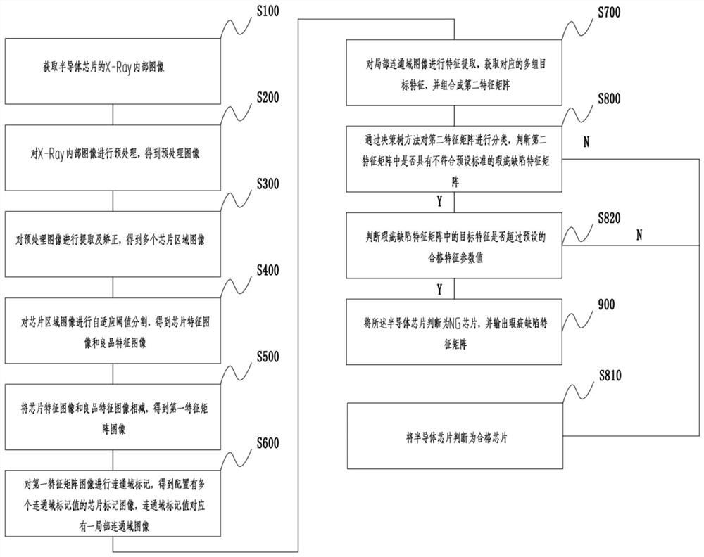
[0062] Such as figure 1 As shown, the chip defect visual inspection method provided in this embodiment includes:

[0063] S100. Acquire the X-Ray internal image of the semiconductor chip; wherein, the X-Ray internal image in this embodiment refers to obtaining the X-Ray image corresponding to a plurality of semiconductor chips placed on the material tray through the X-Ray unit, that is X-Ray internal images include internal imaging of multiple semiconductor chips;

[0064] S200. Perform preprocessing on the X-Ray internal image to obtain a preprocessed image; wherein, the preprocessing refers to performing denoising and other processing on the X-Ray internal image to reduce the amount...

Embodiment 2

[0124] A device provided in this embodiment includes a memory and a processor. The memory stores a control program that can run on the processor. When the control program is executed by the processor, the chip defect visual inspection method in Embodiment 1 is implemented.


PUM


Abstract

The invention discloses a chip defect visual detection method and device, and the method comprises the steps: carrying out the preprocessing, extraction, correction, self-adaptive threshold segmentation and subtraction of a semiconductor chip X-Ray image, obtaining a first feature image, carrying out the connected domain marking and feature extraction of the first feature image, obtaining a second feature matrix, carrying out the classification through a decision tree method, and carrying out the detection of a chip defect. Judging whether the plurality of second characteristic matrixes have flaw defect characteristic matrixes which do not meet the preset standard, positioning flaws and defects and judging whether the flaws and the defects are bad chips or not; in the process, the first feature matrix image is obtained by subtracting the chip feature image from the good product feature image, and the second feature matrix image is classified through the decision tree method to form a unique detection thought with the subtraction method as the core, so that the overall calculation amount is small, the structure is simple and easy to implement, and the detection accuracy is improved. The chip screening efficiency is improved, manual work is replaced, and the chip screening device has the advantages of being high in efficiency, low in cost and the like.

Description

technical field [0001] The invention relates to the technical field of semiconductor chip manufacturing, in particular to a chip defect visual detection method and equipment. Background technique [0002] Semiconductor chip manufacturing belongs to the high-tech field and represents a country's industrial technology development level. Its production efficiency affects the production of downstream electronic products such as notebooks and mobile phones; One of the important detection contents of inspection has a wide range of market application requirements in industrial intelligent manufacturing production. The traditional detection method is to manually detect chip defects. With the complexity and precision of semiconductor chips, the efficiency and reliability of manual detection have changed. It is getting lower and lower, and the cost of manual inspection is also rising, that is, the manual inspection method in the prior art is inefficient, high in cost, and poor in reli...

Claims


Application Information

Patent Timeline
IPC IPC(8): G06T7/00G06T7/136G06T7/187G06T7/60G06T3/00G06T5/00
CPCG06T7/0004G06T7/136G06T7/187G06T7/60G06T2207/10004G06T2207/30148G06T2207/20048G06T2207/20024G06T3/02G06T5/70
Inventor 韦受宁徐同魏承锋徐地华
Owner GUANGDONG ZHENGYE TECH