Method and device for determining area of sub-pixel

A determination method and seed pixel technology, applied in static indicators, instruments, etc., can solve problems such as OLED display panel color shift, pixel circuit drive current increase, pixel circuit color shift, etc., to solve the problem of color shift and avoid temperature Elevated effect

Pending Publication Date: 2022-05-13
SHENZHEN CHINA STAR OPTOELECTRONICS SEMICON DISPLAY TECH CO LTD
View PDF0 Cites 0 Cited by
  • Summary
  • Abstract
  • Description
  • Claims
  • Application Information

AI Technical Summary

Problems solved by technology

[0005] This application proposes a method for determining the area of ​​a sub-pixel and a device for determining the area of ​​a sub-pixel in order to effectively solve the technical defect of the pixel circuit due

Method used


Image

  • Method and device for determining area of sub-pixel
  • Method and device for determining area of sub-pixel
  • Method and device for determining area of sub-pixel

Examples


Example Embodiment

[0045] The technical scheme in the embodiment of the application will be described clearly and completely below in combination with the attached drawings in the embodiment of the application. Obviously, the described embodiments are only part of the embodiments of the application, not all of the embodiments. Based on the embodiments in the application, all other embodiments obtained by those skilled in the art without creative work belong to the scope of protection of the application. In addition, it should be understood that the specific embodiments described herein are only used to illustrate and explain the application and are not used to limit the application.

[0046] In this application, the terms "first", "second" and "third" are only used for descriptive purposes and cannot be understood as indicating or implying relative importance or implicitly indicating the number of indicated technical features. Thus, the features defining "first", "second" and "third" may explicitly ...


PUM


Abstract

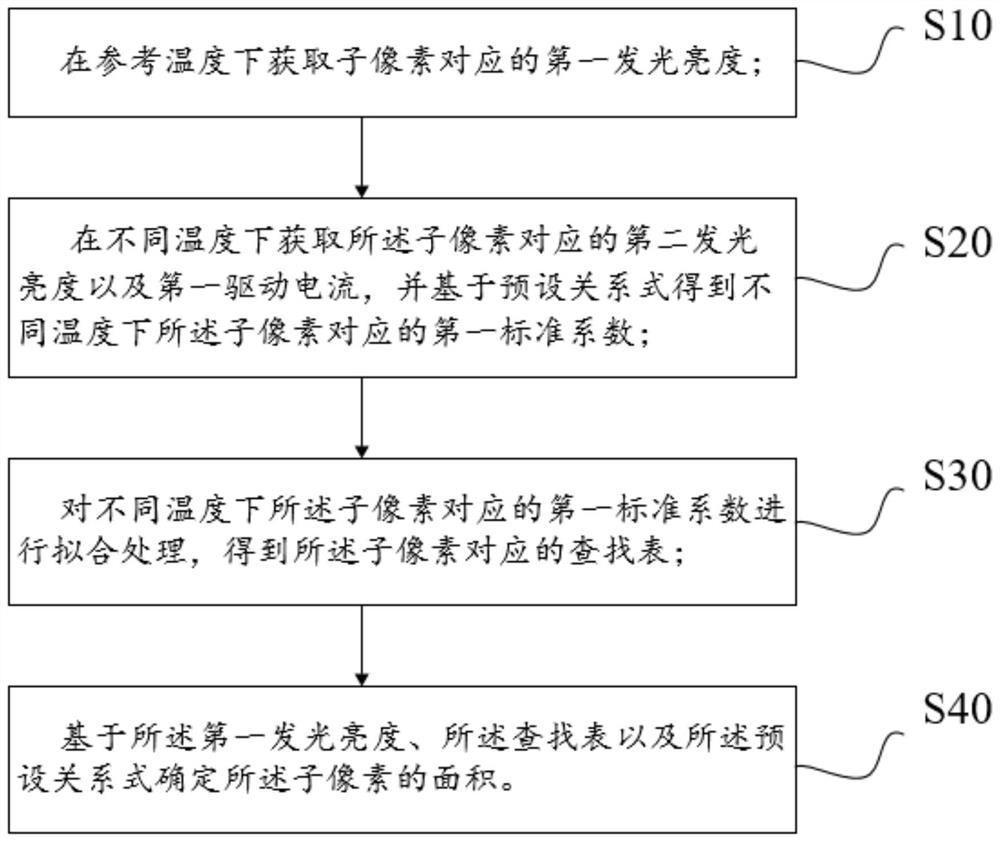
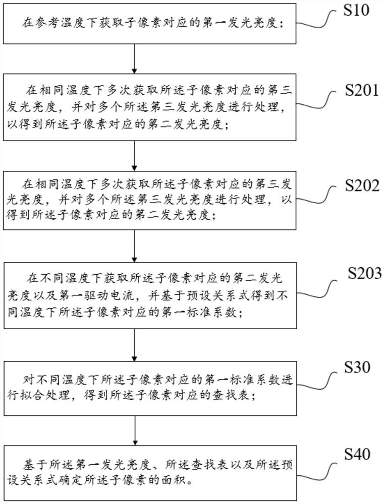
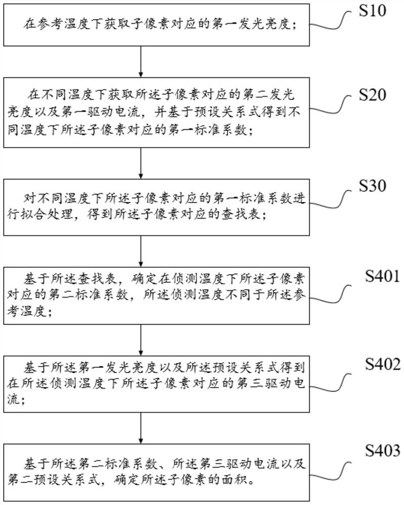
The invention discloses a sub-pixel area determining method and a sub-pixel area determining device. The sub-pixel area determining method comprises the following steps: acquiring first light-emitting brightness corresponding to a sub-pixel at a reference temperature; acquiring a second luminance and a first driving current corresponding to the sub-pixel at different temperatures, and obtaining a first standard coefficient corresponding to the sub-pixel at different temperatures based on a preset relational expression; performing fitting processing on the first standard coefficients corresponding to the sub-pixels at different temperatures to obtain a lookup table corresponding to the sub-pixels; and determining the area of the sub-pixel based on the first luminance, the lookup table and the preset relational expression. According to the invention, the problem of color cast caused by temperature rise of the pixel circuit can be effectively solved, and the uniformity of luminance is improved.

Description

technical field [0001] The present application relates to the field of display technology, in particular to a method for determining the area of ​​a sub-pixel and a device for determining the area. Background technique [0002] Organic Light Emitting Diode (OLED), as a current-mode light-emitting device, has the characteristics of self-luminescence, fast response, wide viewing angle and can be fabricated on flexible substrates, and is increasingly used in high-performance displays. in the field. In the existing OLED display panel, each OLED needs to be driven by its corresponding pixel circuit on the array substrate to emit light to realize display. [0003] However, the long-term operation of the pixel circuit will lead to temperature rise, and then the mobility of the driving transistor of the OLED will increase based on the temperature rise, which will further lead to an increase of the driving current of the OLED. Based on the increase in driving current, the brightnes...

Claims


Application Information

Patent Timeline
IPC IPC(8): G09G3/3283
CPCG09G3/3283G09G2300/0439G09G2320/0233G09G2320/041G09G2320/0242
Inventor 陈媚
Owner SHENZHEN CHINA STAR OPTOELECTRONICS SEMICON DISPLAY TECH CO LTD
Why Eureka
Try Eureka