Semiconductor device and method of manufacturing the same

a semiconductor and semiconductor technology, applied in the field of semiconductor devices, can solve the problems of high cost of semiconductor devices, and the requirement of heat resistance, so as to simplify the wiring pattern and prevent the temperature rise of semiconductor chips

Inactive Publication Date: 2007-04-24
SANYO ELECTRIC CO LTD
View PDF17 Cites 53 Cited by
  • Summary
  • Abstract
  • Description
  • Claims
  • Application Information

AI Technical Summary

Benefits of technology

[0020]As understood from the method of manufacturing a semiconductor as described later, since the bridge and external connecting electrodes are supported by the insulating resin, unlike the prior art, no adhesive tape is required. In addition, since the rear surface of the semiconductor chip is directly mounted a mounting board, a temperature rise in the semiconductor chip can be prevented.
[0021]Secondly, since the rear surface of each of the insulating resin and the bridge is coated with an insulating film, the wirings on the mounting board can be extended to the rear surface of the bridge, thereby simplifying the wiring pattern on the side of the mounting board.

Problems solved by technology

However, the adhesive tape 13, to which heat is applied during molding, is required to have heat resistance and hence expensive.
This leads to cost up of the semiconductor device.
However, adoption of the supporting board increases the thickness of the semiconductor device, and so leads to cost up thereof.
This leads to temperature rise of the semiconductor chip.
This makes it impossible to bring out the inherent capability of the semiconductor chip.

Method used


Image

  • Semiconductor device and method of manufacturing the same
  • Semiconductor device and method of manufacturing the same
  • Semiconductor device and method of manufacturing the same

Examples


embodiment 1

[0041 explaining the semiconductor device according to the invention.

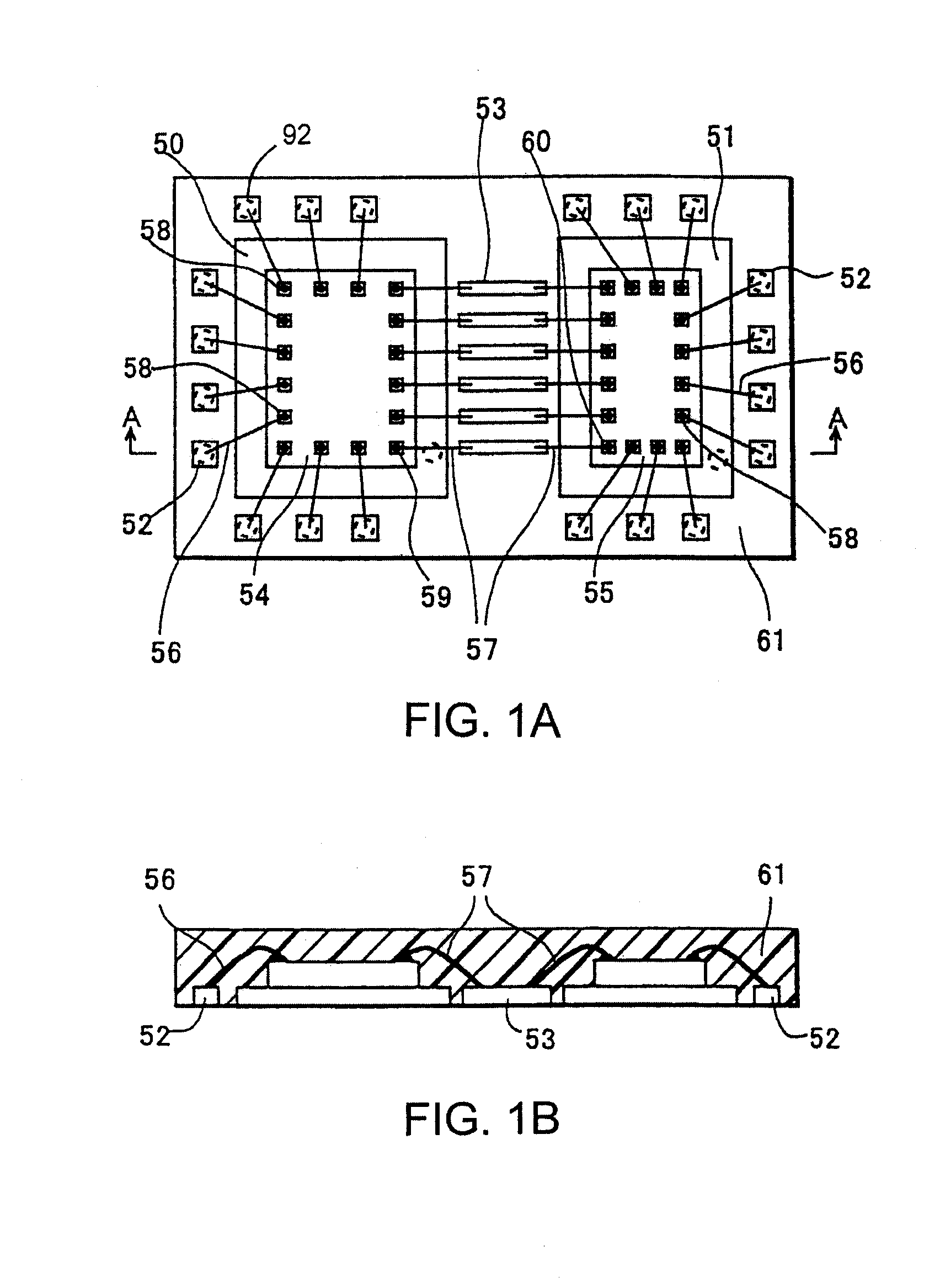
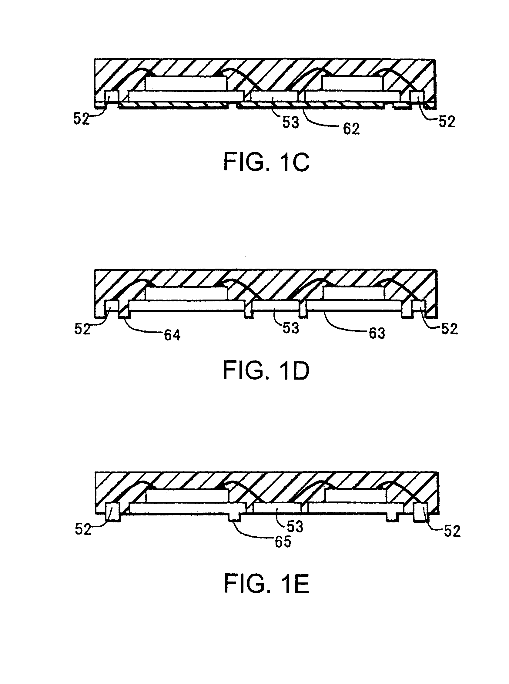
[0042]FIG. 1A is a plan view of a semiconductor device according to the invention. FIGS. 1B–1E are sectional views taken in line A—A in FIG. 1A. FIGS. 1B–1E show four types of the rear-surface structure of the semiconductor device.

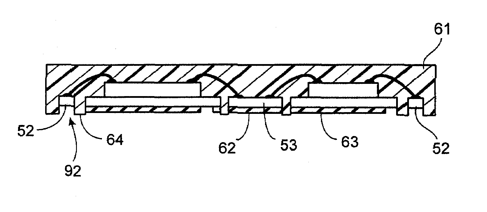
[0043]In this invention, a first die pad 50 and a second die pad 51 are arranged on substantially the same plane, and external connecting electrodes 52 are formed around them. The front surface of each of the connecting electrodes 52 serves as a bonding pad whereas the rear surface thereof is externally connected. At least one bridge 53 is formed between the first die pad 50 and the second die pad 51.

[0044]A first semiconductor chip 54 is fixed onto the first die pad 50, whereas a second semiconductor chip 55 is fixed onto the second die pad 51. These semiconductor chips 54 and 55 are connected to each other by metallic wires.

[0045]The metallic wires include a first metallic wire 56 conne...

embodiment 2

[0057 explaining the semiconductor device according to the invention.

first embodiment

[0058]FIG. 2A is a plan view of a semiconductor device according to the invention. FIGS. 2B–2E are sectional views taken in line A—A in FIG. 2A. FIGS. 2B–2E show the rear-surface structures of the semiconductor device like the

[0059]The feature of this embodiment resides in that the semiconductor chips 54, 55 for face-down are adopted so that the external connecting electrodes 52 can be arranged immediately below the semiconductor chip, thereby reducing the planar area and thickness of the semiconductor device.

[0060]Each of the first semiconductor chip 54 and the second semiconductor chip 55 may be a bare chip, a flip-chip, SMD, a wafer scale CSP, etc. The external connecting electrodes 52 are formed at the positions corresponding to the electrodes on the semiconductor chips 54, 55. The external connecting electrodes 52 and electrodes of the semiconductor chips 54, 55 are connected to each other by connecting means. This connecting means may be an Au bump, brazing material, soldering...


PUM


Abstract

Die pads 50, 51, an external connecting electrode 52 and a bridge are covered with an insulating resin after half-etching, formed into a single package without a coupling member such as a supporting lead or adhesive tape. In addition, since no supporting board is required, a low-profile semiconductor device with improved heat radiation can be provided.

Description

BACKGROUND OF THE INVENTION[0001]1. Field of the Invention[0002]This invention relates to a semiconductor device and a method of manufacturing it, and more particularly to a semiconductor device in which a plurality of semiconductor chips are mounted a planar or superposed manner and a method of manufacturing it.[0003]2. Description of the Related Art[0004]In recent years, in order to increase the capacity of a memory and also extend the circuit function, a plurality of chips are mounted in a single package.[0005]For example, as shown in FIG. 12, a semiconductor device 3 with two semiconductor chips 1 and 2 arranged two-dimensionally is mounted in a single package. The semiconductor device 3 is formed in a lead frame in which a large number of leads 6 are arranged around a first die pad 4 and a second die pad 5. Bridges 7 are arranged between the first die pad 4 and the second die pad 5. The first semiconductor chip 1 is fixed onto the first die pad 4, whereas the second semiconduct...

Claims


Application Information

Patent Timeline
Patent Type & Authority Patents(United States)
IPC IPC(8): H01L23/24H01L23/22H01L21/48H01L25/18H01L23/31H01L23/495H01L25/04H01L25/065H01L25/07
CPCH01L21/4828H01L23/3107H01L23/49548H01L23/49575H01L24/49H01L24/97H01L25/0652H01L21/4832H01L2924/07802H01L2224/16245H01L2224/32014H01L2224/32145H01L2224/48091H01L2224/48247H01L2224/48465H01L2224/4903H01L2224/49051H01L2224/49113H01L2224/49171H01L2224/49175H01L2224/73265H01L2224/97H01L2924/01004H01L2924/01006H01L2924/01013H01L2924/01028H01L2924/01029H01L2924/01046H01L2924/01047H01L2924/01079H01L2924/01082H01L2924/19041H01L2924/30105H01L24/48H01L2924/014H01L2924/01033H01L2924/00014H01L2924/00H01L2224/451H01L2924/15787H01L2224/05599H01L2224/85399H01L2924/181H01L2224/05554H01L2924/00015H01L2224/45015H01L2924/207H01L2924/00012H01L2224/45099
Inventor SAKAMOTO, NORIAKIOCHIAI, ISAO
Owner SANYO ELECTRIC CO LTD
Why Eureka
Try Eureka