Multilayer circuit board and manufacturing method thereof

A technology for a multilayer circuit board and a manufacturing method, which is applied in the directions of multilayer circuit manufacturing, printed circuit components, and structural connection of printed circuits, can solve problems such as complex methods and unfavorable efficiency, achieve simple and convenient preparation, and improve combination efficiency. , to avoid the effect of the disassembly step

Pending Publication Date: 2022-07-08
QING DING PRECISION ELECTRONICS HUAIAN CO LTD +1
View PDF0 Cites 0 Cited by
  • Summary
  • Abstract
  • Description
  • Claims
  • Application Information

AI Technical Summary

Problems solved by technology

However, the above method is relatively complicated, which is not conducive to improving the efficiency

Method used


Image

  • Multilayer circuit board and manufacturing method thereof
  • Multilayer circuit board and manufacturing method thereof
  • Multilayer circuit board and manufacturing method thereof

Examples


Embodiment Construction

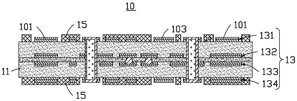
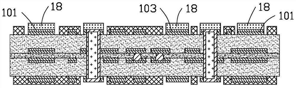
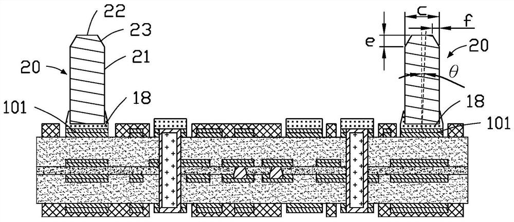
[0025] The technical solutions in the embodiments of the present application will be clearly and completely described below with reference to the accompanying drawings in the embodiments of the present application. Obviously, the described embodiments are only a part of the embodiments of the present application, rather than all the embodiments. Based on the embodiments of the present invention, all other embodiments obtained by those of ordinary skill in the art without creative efforts shall fall within the scope of protection of the present application.

[0026] It should be noted that when an element is referred to as being "fixed to" another element, it can be directly on the other element or intervening elements may also be present. When an element is referred to as being "connected" to another element, it can be directly connected to the other element or intervening elements may also be present. When an element is referred to as being "disposed on" another element, it c...


PUM

PropertyMeasurementUnit
Spacingaaaaaaaaaa

Abstract

A manufacturing method of a multilayer circuit board comprises the following steps that a first circuit substrate is provided, and one side of the first circuit substrate is provided with at least two spaced first welding pads and at least one second welding pad; solder paste is arranged on the first welding pad and the second welding pad; each first welding pad is welded with a positioning column through solder paste on the first welding pad; a second circuit substrate is provided, one side of the second circuit substrate is provided with at least one third welding pad, and at least two through holes penetrate through the second circuit substrate; solder paste is arranged on the third welding pad; the first circuit substrate and the second circuit substrate are stacked, each positioning column penetrates through one through hole, and each second welding pad corresponds to one third welding pad and makes contact with the third welding pad through solder paste; and welding the second welding pad and the third welding pad through reflow soldering. The manufacturing method is convenient for improving the efficiency. The invention also relates to a multilayer circuit board.

Description

technical field [0001] The invention relates to the field of circuit boards, in particular to a multi-layer circuit board and a manufacturing method thereof. Background technique [0002] When designing circuit boards, modular design has been widely used. In order to meet the different needs of the market, different functional hardware circuits are designed on different circuit board modules, and different products are formed through the selection and combination of modules. In the prior art, two circuit board modules are usually positioned by means of a positioning fixture and CCD alignment, so as to facilitate subsequent fixing of the two circuit board modules. However, the above method is relatively complicated, which is not conducive to improving the efficiency. SUMMARY OF THE INVENTION [0003] In view of this, the present invention provides a method for manufacturing a multi-layer circuit board with improved efficiency. [0004] Also provided is the above-mentioned...

Claims


Application Information

Patent Timeline
IPC IPC(8): H05K3/46H05K1/14
CPCH05K3/4679H05K3/4644H05K1/144
Inventor 黎耀才李彪钟浩文
Owner QING DING PRECISION ELECTRONICS HUAIAN CO LTD
Why Eureka
Try Eureka