Electronic cart for wafer carrying

A trolley and electronic technology, applied in trolleys, multi-axis trolleys, trolley accessories, etc., can solve problems affecting production efficiency and lack of information, and achieve timely and accurate reading and writing

Pending Publication Date: 2022-07-12
江苏道达智能科技有限公司
View PDF8 Cites 0 Cited by
  • Summary
  • Abstract
  • Description
  • Claims
  • Application Information

AI Technical Summary

Problems solved by technology

[0003] There are many links in the manufacturing process of semiconductor wafers. It is necessary to turn over the wafers through the wafer box. Since the whole process cannot be monitored in the logistics link, there is a lack of information, especially the delivery of wafer boxes. process, resulting in the need for retrospective checks, affecting production efficiency

Method used


Image

  • Electronic cart for wafer carrying
  • Electronic cart for wafer carrying

Examples


Embodiment Construction

[0021] The present invention will be further described below with reference to the accompanying drawings and specific embodiments, so that those skilled in the art can better understand the present invention and implement it, but the embodiments are not intended to limit the present invention.

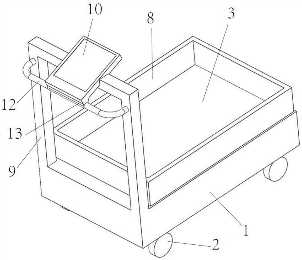
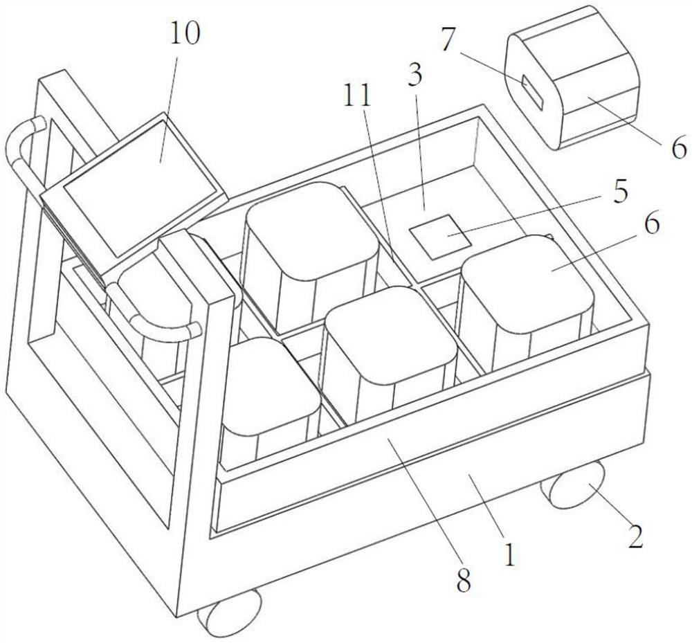
[0022] refer to figure 1 As shown, an embodiment of the electronic cart for wafer handling of the present invention includes a mobile platform 1, the bottom of the mobile platform is provided with a shock-absorbing wheel 2, the surface of the mobile platform is provided with a bearing platform 3, and the bottom of the bearing platform is also provided with a The reader 5, the surface of the bearing platform is used to place the wafer cassette 6, and the wafer cassette is provided with an electronic label 7, and the information on the electronic label can be read and written through the reader, so as to obtain the information of the wafers in the wafer cassette, Including parameters suc...


PUM


Abstract

The invention discloses an electronic cart for wafer carrying, which comprises a mobile platform, damping wheels are arranged at the bottom of the mobile platform, a bearing platform is arranged on the surface of the mobile platform, a weighing sensor is arranged between the mobile platform and the bearing platform, and a reader is further arranged at the bottom of the bearing platform. The surface of the bearing platform is used for placing a wafer box, an electronic tag is arranged on the wafer box, a fence is further arranged on the portion, on the periphery of the bearing platform, of the movable platform, a push-pull handrail is arranged on one side of the movable platform, and a display module is arranged on the push-pull handrail. A battery and a controller are arranged in the mobile platform, the controller is connected with the reader, the weighing sensor and the display module, and the battery supplies power to the weighing sensor, the reader, the display module and the controller. The effect of transmitting materials and corresponding information in the conveying process can be achieved, and the production efficiency is improved.

Description

technical field [0001] The invention relates to the technical field of semiconductor manufacturing, in particular to an electronic cart used for wafer handling. Background technique [0002] Wafers are the basic raw materials for the manufacture of semiconductor devices. Ultra-high purity semiconductors are prepared into wafers through crystal pulling, slicing and other processes. The wafers undergo a series of semiconductor manufacturing processes to form extremely tiny circuit structures, which are then cut, packaged, and tested to become chips, which are widely used in various electronic equipment. . [0003] There are many links in the manufacturing process of semiconductor wafers. It is necessary to turn the wafers through the wafer box. Since the whole process cannot be monitored in the logistics link, there is a lack of information, especially the transportation of the wafer box. In the process, it leads to the need for retrospective verification, which affects the ...

Claims


Application Information

Patent Timeline
Patent Type & Authority Applications(China)
IPC IPC(8): B62B3/00B62B5/00G01G19/12G06K17/00
CPCB62B3/00B62B3/005B62B5/0003G01G19/12G06K17/00
Inventor 曹旭东孙俊杰付斌
Owner 江苏道达智能科技有限公司
Why Eureka
Try Eureka