Wafer defect detection optimization method and device

A defect detection and optimization method technology, which is applied in the semiconductor field, can solve the problems of low sampling coverage and achieve the effect of improving sampling efficiency and sampling coverage

Inactive Publication Date: 2022-08-02
SOI MICRO CO LTD +1
View PDF0 Cites 2 Cited by
  • Summary
  • Abstract
  • Description
  • Claims
  • Application Information

AI Technical Summary

Problems solved by technology

The inspection method of sampling wafer boxes cannot meet the problem of machine cavity, and the coverage rate of sampling inspection is low, which is prone to hidden risks

Method used


Image

  • Wafer defect detection optimization method and device
  • Wafer defect detection optimization method and device
  • Wafer defect detection optimization method and device

Examples


Embodiment Construction

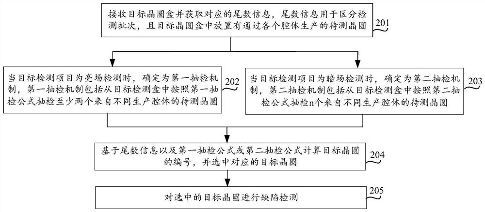
[0016] In order to make the objectives, technical solutions and advantages of the present application clearer, the embodiments of the present application will be further described in detail below with reference to the accompanying drawings.

[0017] As used herein, "plurality" refers to two or more. "And / or", which describes the association relationship of the associated objects, means that there can be three kinds of relationships, for example, A and / or B, which can mean that A exists alone, A and B exist at the same time, and B exists alone. The character " / " generally indicates that the associated objects are an "or" relationship.

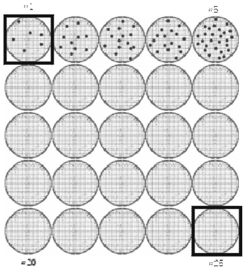
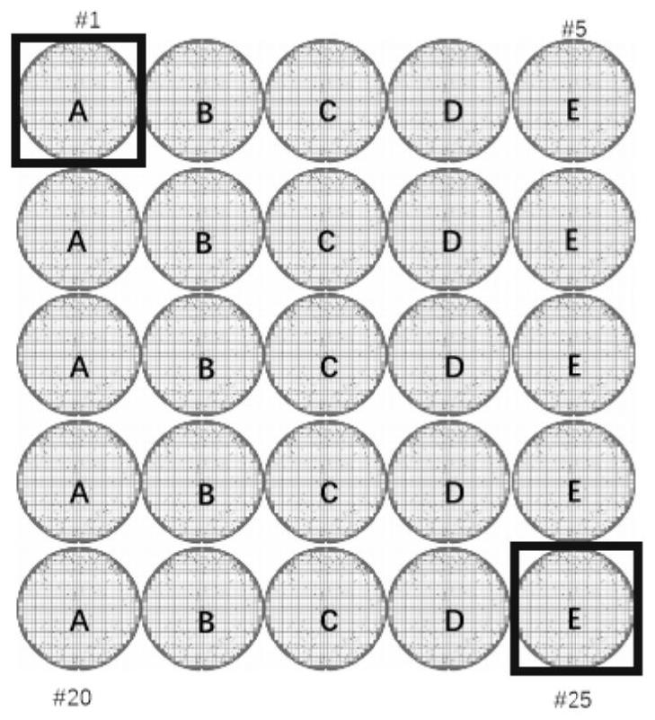
[0018] in related technologies such as figure 1 As shown, there are 25 wafers to be tested in the wafer cassette. These wafers to be tested are from different cavities of the production machine. The wafer batches produced in different cavities may have differences in accuracy and quality. The defect detection at the stage is to select the corr...


PUM


Abstract

The embodiment of the invention discloses a wafer defect detection optimization method and device, and relates to the technical field of semiconductors, and the method comprises the steps: receiving a target wafer box and obtaining corresponding mantissa information, the mantissa information is used for distinguishing detection batches, and to-be-detected wafers produced through all cavities are placed in the target wafer box; determining a target detection item of the target wafer box, and carrying out spot check on target wafers with corresponding numbers from the target wafer box according to the target detection item, a corresponding wafer spot check mechanism and mantissa information; wherein different detection items correspond to different wafer sampling inspection mechanisms, and the wafer sampling inspection mechanisms are used for determining and calculating the number and mark numbers of sampling inspection wafers; and performing defect detection on the selected target wafer.

Description

technical field [0001] Embodiments of the present application relate to the field of semiconductor technology, and in particular, to a method and device for optimizing wafer defect detection. Background technique [0002] In the integrated circuit process, after the wafer is produced in the inner cavity of the machine, it needs to be tested for defects. . [0003] In the related art, the defect detection of wafers is carried out by sampling the wafer cassette for passing-through detection, or by sampling the wafers with fixed numbers in the wafer cassette. The inspection method of spot-checking wafer cassettes cannot consider the problem of the machine cavity again, and its sampling coverage rate is low, which is prone to hidden risks. SUMMARY OF THE INVENTION [0004] Embodiments of the present application provide a method and device for optimizing wafer defect detection. The technical solution is as follows: [0005] In one aspect, a method for optimizing wafer defec...

Claims


Application Information

Patent Timeline
Patent Type & Authority Applications(China)
IPC IPC(8): H01L21/66
CPCH01L22/12H01L22/20Y02P90/30
Inventor 张简志胜叶甜春陈少民李彬鸿
Owner SOI MICRO CO LTD
Why Eureka
Try Eureka