
Variable inductor element

An inductive element, variable technology, applied in the direction of electrical components, variable inductance/transformers, inductors, etc., can solve the problems of increasing the wrong cutting of the horizontal strip 71b, narrowing the interval of the horizontal strip 71b, and difficulty in adjusting the inductance

Inactive Publication Date: 2004-07-21
MURATA MFG CO LTD
View PDF0 Cites 0 Cited by
  • Summary
  • Abstract
  • Description
  • Claims
  • Application Information

AI Technical Summary

Problems solved by technology

However, in the inductance element 75, as the number of cut lateral bars 71b increases, the intervals of the lateral bars 71b become narrower.
This increases the possibility of the transverse strip 71b being cut incorrectly, causing a problem of difficulty in inductance adjustment

Method used


Image

  • Variable inductor element
  • Variable inductor element
  • Variable inductor element

Examples


Embodiment Construction

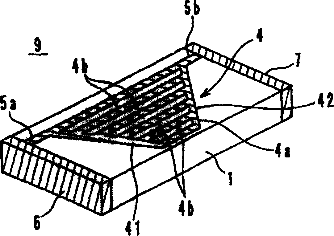
[0019] Embodiments of the variable inductance element of the present invention will be described below with reference to the drawings.

[0020] like figure 1 As shown, after the upper surface of the insulating substrate 1 is ground to a smooth surface, the inductor pattern 4 is formed on the upper surface of the insulating substrate 1 using a thick film printing method or a thin film forming method such as photolithography or the like. According to the thick film printing method, a mask with openings at the desired pattern is made, covered on the upper surface of the insulating substrate 1, and an electrically conductive paste is applied from the top of the mask, so that the openings through the mask A conductor having a relatively large thickness is formed on the exposed upper surface of the insulating substrate 1 in a desired pattern (inductor pattern 4 in this embodiment).

[0021] An example of photolithography will be described below. A relatively thin conductive film ...


PUM


Abstract

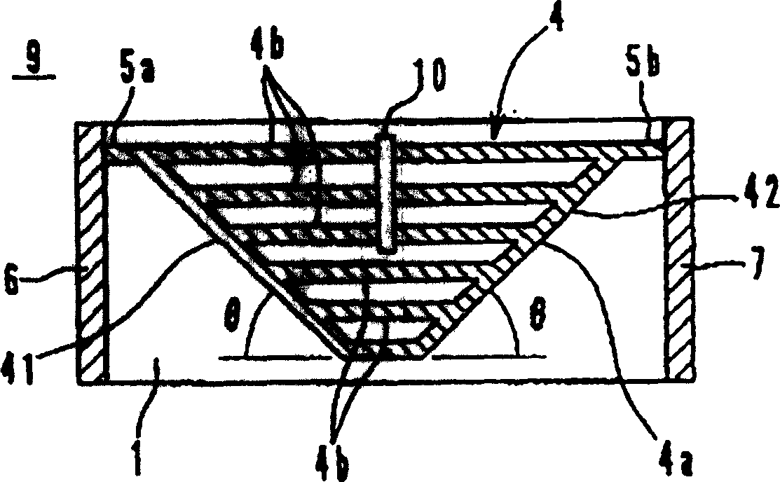
An inductor pattern is formed on the upper face of an insulating substrate. The inductor pattern is a ladder-shaped electrode composed of a substantially V-shaped frame portion and plural lateral bars crossing across two arms of the substantially V-shaped frame portion to be trimmed for adjustment of the inductance. The plural lateral bars are arranged at substantially equal intervals. The two arms of the substantially V-shaped frame portion have an angle of 45 DEG approximately to the lateral bars.

Description

technical field [0001] The present invention relates to variable inductance elements, and in particular, to variable inductance elements for use particularly in mobile communication devices, such as mobile phones and the like. Background technique [0002] In recent years, mobile communication devices, such as portable telephones, etc. have been remarkably miniaturized, and there has been a strong demand to reduce the size of electronic components used in these devices. In addition, as higher frequencies are used in mobile communication devices, the circuits of these devices become more complex, and in addition, the characteristics of electronic components to be mounted in these devices need to be consistent and highly accurate. [0003] However, in order to be able to perform the desired function in some cases, for the formation of the circuit, even if each electronic component has uniform characteristics and high-precision parameters, the deviation in the parameter of each...

Claims


Application Information

Patent Timeline
Patent Type & Authority Patents(China)
IPC IPC(8): H01F21/00H01F17/00H01F21/12H01F41/04H01P3/08
CPCH01F21/00Y10T29/4902H01P3/088H01F41/045H01F17/0006
Inventor 饭田直树川口正彦
Owner MURATA MFG CO LTD
Learn More