Optical Pick-up device
An optical pick-up device and laser beam technology, applied in the direction of beam guiding device, beam source, optical detector, etc., can solve the problems of mass production cost, difficult device adjustment, complex structure, etc.
- Summary
- Abstract
- Description
- Claims
- Application Information
AI Technical Summary
Problems solved by technology
Method used
Image

Examples
Embodiment Construction
[0025] Embodiments of the present invention will be described in detail below with reference to the accompanying drawings.
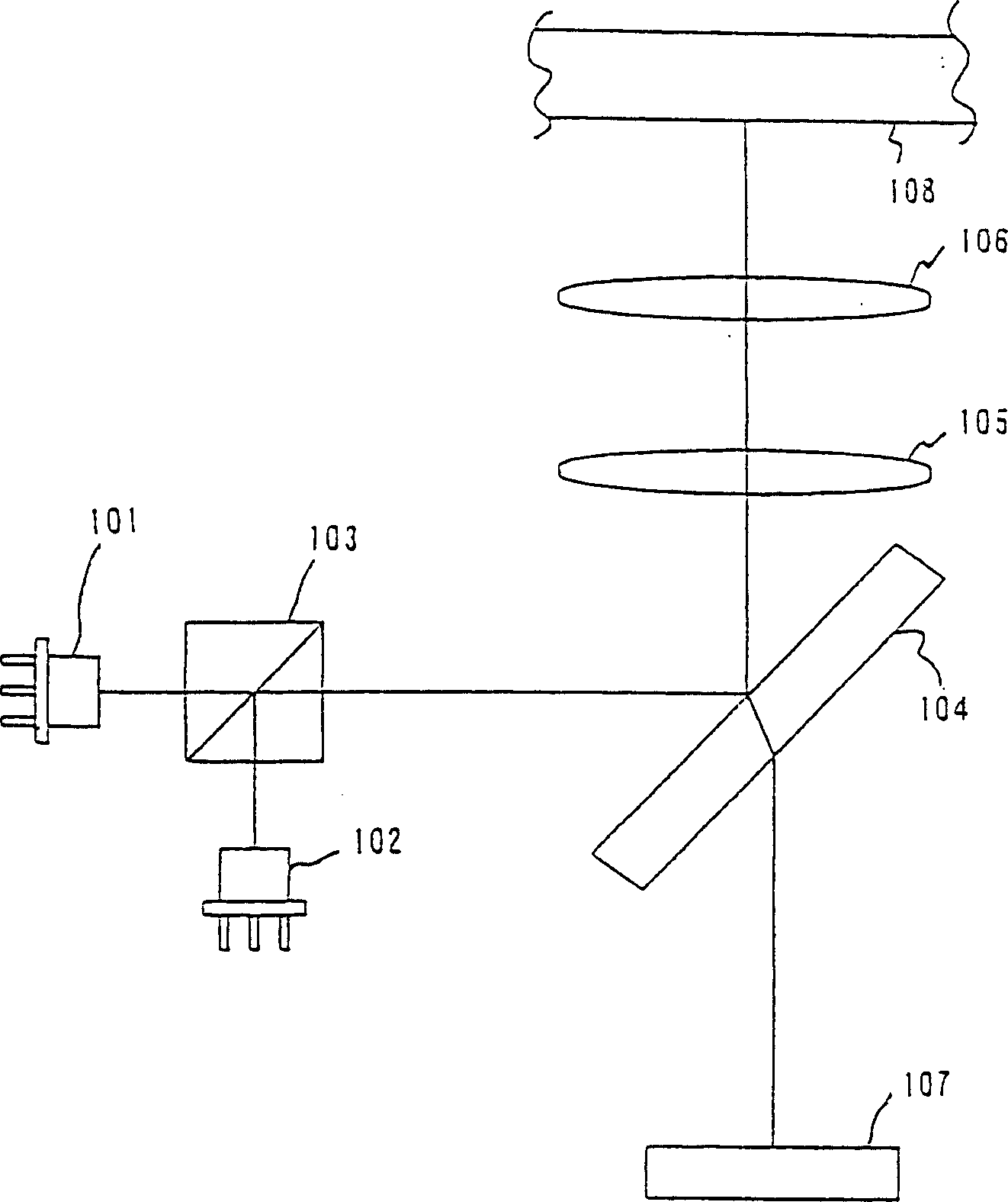
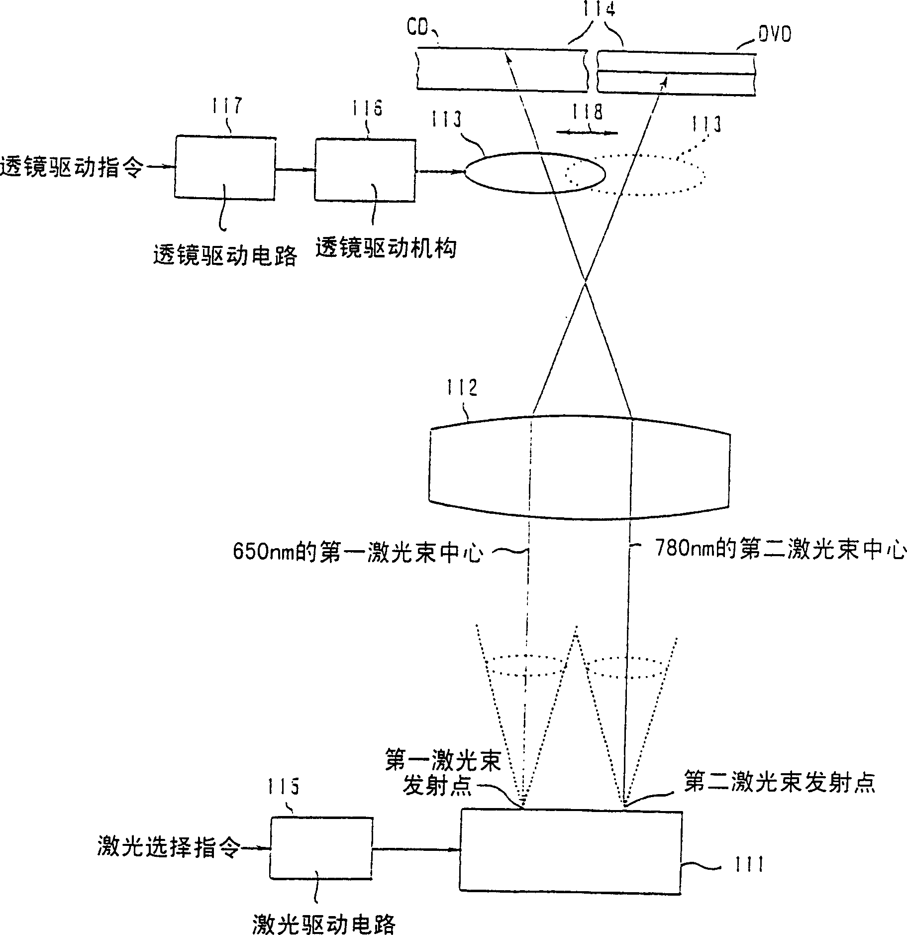
[0026] figure 2 The optical system of the optical pickup device according to the present invention is schematically shown. The optical pickup has a semiconductor laser device 111 for emitting laser beams of two different wavelengths. The semiconductor laser device 111 independently emits a first laser beam with a wavelength of 650 nm and a second laser beam with a wavelength of 780 nm from different light emitting points in the same emission direction. The interval L between the light emitting points is about 100 μm.
[0027] The optical pickup device is configured so that the laser beam emitted from the semiconductor laser device 111 passes through the collimator lens 112 and the objective lens 113 in order and reaches the optical disc 114 . DVDs and CDs (including CD-Rs) are used as the optical disc 114, and one of the used discs is placed on a tur...
PUM
 Abstract
Description
Claims
Application Information