Static discharge protecting element and realated circuit

A technology for electrostatic discharge protection and electrostatic discharge detection, which is applied in electrical components, circuits, and electrical solid devices, etc., and can solve problems such as long current paths and difficulty in quickly discharging ESD currents.

Inactive Publication Date: 2004-09-15
VANGUARD INTERNATIONAL SEMICONDUCTOR CORPORATION
View PDF0 Cites 1 Cited by
  • Summary
  • Abstract
  • Description
  • Claims
  • Application Information

AI Technical Summary

Problems solved by technology

and figure 1 Comparing the ESD current path in the, figure 2 The current path in is significantly longer, so, relatively, figure 2 LVTSCR manufactured by China-Israel STI manufacturing process will be difficult to quickly discharge ESD current

Method used


Image

  • Static discharge protecting element and realated circuit
  • Static discharge protecting element and realated circuit
  • Static discharge protecting element and realated circuit

Examples


Embodiment Construction

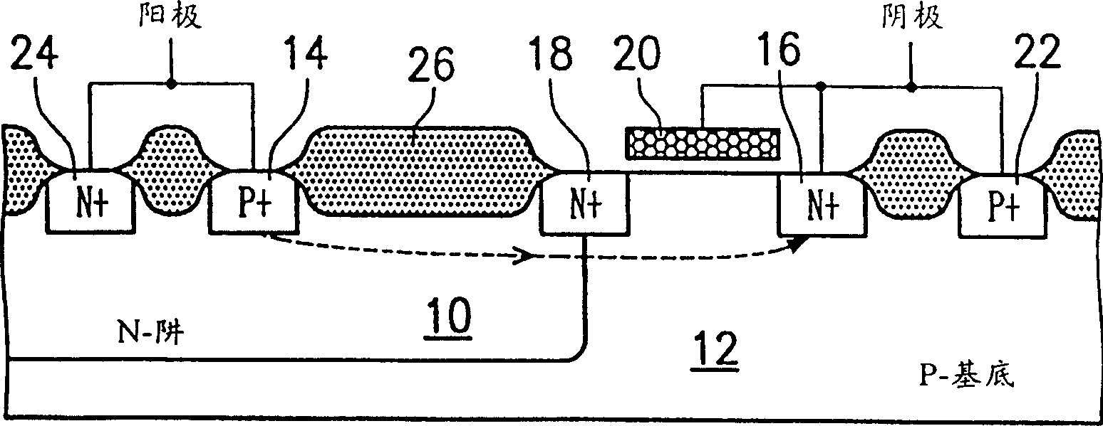
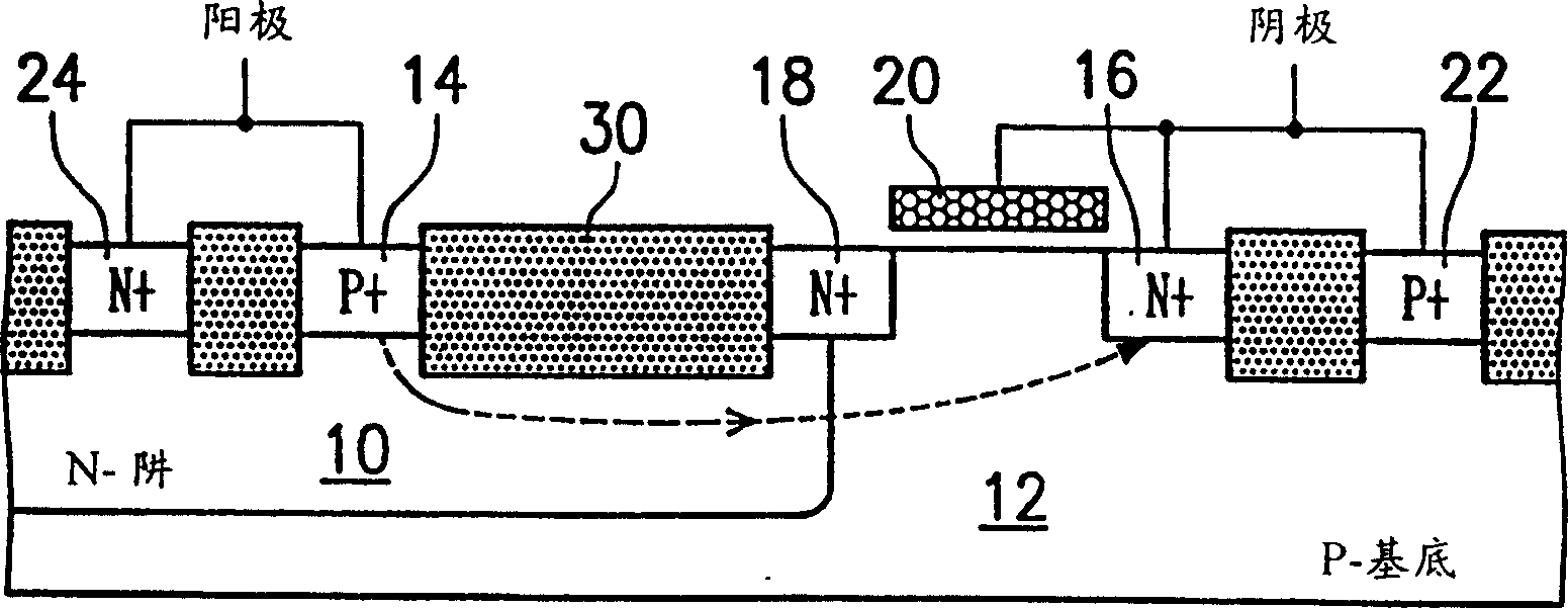
[0024] The spirit of the present invention is to use a redundant gate structure to replace the STI layer through which the ESD current in the known LVTSCR must bypass. In this way, the redundant gate structure can provide the isolation effect of the doped region on the one hand, and on the other hand, does not It will hinder the discharge path of the ESD current when an ESD event occurs. Therefore, the turn-on speed and ESD tolerance of the LVTSCR are improved.

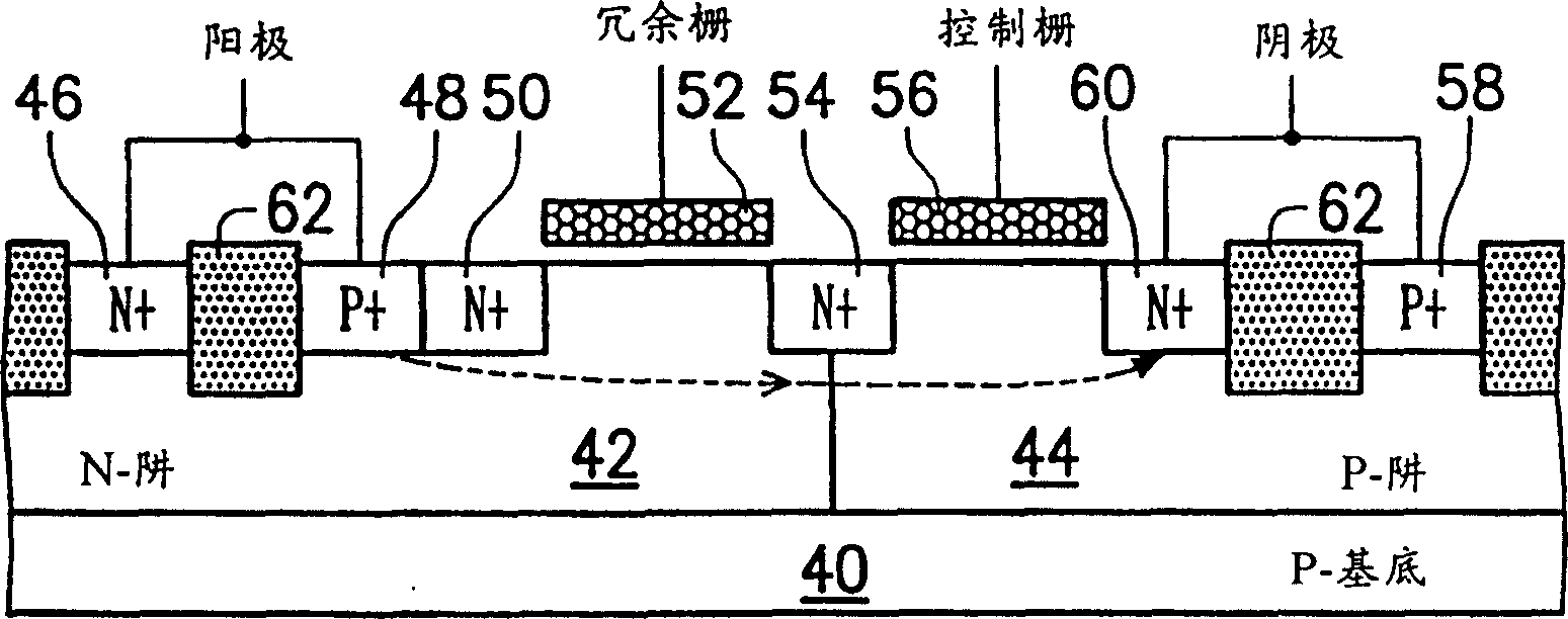
[0025] refer to Figure 3a as well as Figure 3b , Figure 3a For an NMOS-triggered LVTSCR according to the present invention, Figure 3b for Figure 3a The circuit represents the symbol. Figure 3a The LVTSCR in LVTSCR is triggered by an NMOS, referred to as nSCR. The nSCR is fabricated on a P-type substrate 40 and includes an N-type well 42 and a P-type well 44 .

[0026] A P+ doped region 58 is disposed in the P-type well 44 as an electrical contact point of the P-type well 44 . The NMOS for triggering is a...


PUM


Abstract

The invention discloses an ESD and relevent ESD prevention circuit. In the invented ESD prevention element, the redundant grid structure, replaces STT layer that the ESD current must bypass through in well known LVTSCR. Thus in one hand, the redundant grid structure can provide insulation effect in adulteration area, in other hand, it does not block the discharging path when ESD event occurs so as to raise the turning on speed of LVTSCR and tolerance.

Description

technical field [0001] The invention relates to a low-voltage triggering semiconductor control rectifier (Low-voltageTriggering semiconductor control rectifier, LVTSCR) and related circuits, in particular to an LVTSCR and a circuit suitable for a shallow trench isolation (shallow trench isolation, STI) manufacturing process . technical background [0002] With the advancement of manufacturing process technology, electrostatic discharge (ESD) has become one of the main considerations for the reliability of integrated circuits (ICs). Especially after semiconductor manufacturing technology enters the deep submicron regime, scaled-down transistors and thinner gate oxide layers are relatively vulnerable to ESD stress. Therefore, an ESD protection circuit must be provided at the input and output terminals of the IC to protect the components in the IC from being damaged by ESD. [0003] refer to figure 1 , figure 1 It is a cross-sectional view of a traditional LVTSCR. figure 1...

Claims


Application Information

Patent Timeline
Patent Type & Authority Patents(China)
IPC IPC(8): H01L23/60
Inventor 柯明道林耿立
Owner VANGUARD INTERNATIONAL SEMICONDUCTOR CORPORATION
Why Eureka
Try Eureka